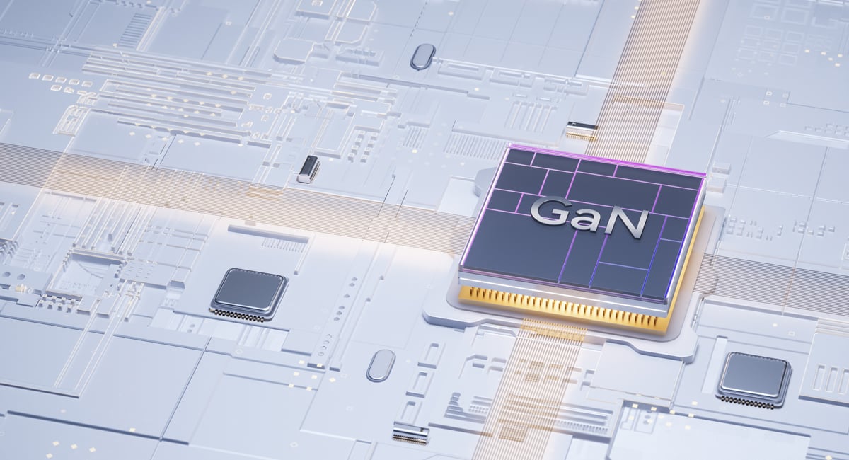
Sarcina Technology has announced the development of patented methodologies for the UCIe-A (Universal Chiplet Interconnect Express-Advanced) and UCIe-S (Standard) protocols. The company’s latest innovations include an optimised RDL (redistribution layer) interposer design for die-to-die interconnections, supporting data rates up to 32 gigabits transfers per second (GT/s) whilst optimising signal routing architecture to minimise crosstalk and maximise signal integrity.
As AI workloads continue to expand at an unprecedented pace, the semiconductor industry faces the dual challenge of performance and manufacturability. Traditional SoCs are approaching their limits in terms of size, yield, and cost. The solution lies in chiplet-based architectures. Sarcina Technology is focused on enabling package design to achieve the system level performance required for next-generation AI systems.
According to Larry Zu, CEO, Sarcina Technology: “One of the key challenges we are addressing is how to arrange interconnected wires to minimise signal crosstalk and enhance signal integrity. Given the constraints in available space and manufacturing limitations – such as the number of copper layers that can be used – this is a complex problem.”
Zu continues: “Extensive electromagnetic simulations confirm that Sarcina’s novel interposer solutions meet stringent insertion loss and crosstalk requirements, enabling robust, high-bandwidth communication for next-generation AI accelerators and high-performance computing (HPC) systems.”
Sarcina’s patented methodology for the Universal Chiplet Interconnect Express-Advanced (UCIe-A) protocol, using RDL interposers, delivers:
- 32 GT/s die-to-die data rates fully compliant with UCIe 2.0 specifications
- Optimised routing architecture that dramatically reduces crosstalk
- Maximum utilisation of 3D space, with routing channels strictly confined at the die edge (“beach front”) for seamless integration of UCIe-A IP
- Multi-dimensional routing optimisations for data, clock, and redundancy signals, enabling an ultra-compact 3D routing region at the beach front
- Cost-efficient designs that minimise RDL routing layers while staying within current manufacturable limits
- Standardised RDL layouts that improve fabrication yield and streamline manufacturing
Sarcina also leads with UCIe-S (Standard) interconnect methodologies, targeting organic substrates, and advanced PCBs with HDI technology. These substrate-level designs achieve:
- Minimal insertion loss and crosstalk enabling long channel lengths over standard organic substrates
- Structured multi-layer routing confined to an ultra-compact 3D space, allowing dense stacking of UCIe-S modules along the die edge without occupying external routing area
- Compatibility with package-to-package links over organic substrates or HDI PCBs, scalable to PCIe daughter cards, acceleration modules, and system baseboards
- Verified 32 GT/s performance through advanced 3D HFSS, paving the way for UCIe 3.0 adoption
- Seamless die-to-die communication even with silicon transmitter and receiver equalizations disabled, eliminating extra transistor circuit power consumption
By unifying UCIe-A and UCIe-S capabilities, Sarcina provides a comprehensive design and simulation platform for chiplet interconnects across interposers, substrates and PCBs. This allows customers to:
- Partition monolithic SoCs into chiplets for higher yield and cost-efficiency
- Integrate heterogeneous technologies (compute, memory, analog, I/O) across process nodes
- Incorporate silicon photonic dice and fibre array units (FAUs) with compute chiplets in a Co-Packaged Optics package, eliminating data bottlenecks that leave AI compute engines idle
- Deploy scalable, manufacturable, and high-performance solutions for AI acceleration and data-intensive computing
Zu concludes: “At Sarcina, we are not just designing interconnects – we are helping to build the foundation of next-generation AI systems. When customers review our designs, they quickly recognise the value that Sarcina’s package design brings to their AI chip. The advantages are immediately clear: enhanced performance, minimal silicon area, reduced cost, power-efficiency, and ease of manufacturing. These latest innovations enable us to provide our customers with the very best package design.”