The miniaturisation trend requires printing ultra-thin and highly conductive interconnects on complex 3D topographies and heterogeneous substrates. XTPL’s printing technology tackles these challenges. We demonstrate Ultra-Precise Deposition (UPD), a versatile approach to printing micrometric conductive and non-conductive structures on various rigid and flexible substrates (see: https://doi.org/10.1038/s41598-022-13352-5). UPD allows maskless deposition of highly-concentrated silver, copper, and gold pastes, up to 85 wt. % of solid content. The printed feature size can be as small as 1µm, and the maximum electrical conductivity obtained in this range is around 45% of the bulk material.
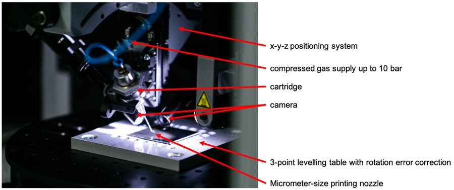 The UPD process is based on a direct extrusion of ink using pressure. Simultaneous optimisation of the ink, printing nozzle and process parameters allows for extrusion of high viscosity inks using nozzles with a diameter as small as 1µm
Thanks to these features, UPD allows to achieve results beyond the reach of other AM techniques: 1) printing on 3D topographies for advanced packaging; 2) printing structures for high-frequency signals, for example, antennas on chip and 5G/6G communication; 3) printing flexible devices, like sensors, using both high and low viscosity materials (10-2.5M cP) with a wide range of feature size (1-200 µm linewidth).
Advanced packaging: printing on 3D topographies
Challenge: printing on vertical sidewalls
The possibility of printing 3D interconnections is particularly interesting for system integration and packaging, including hybrid electronics (combining printed and silicon technologies). For example, we print repeatable and continuous silver lines with a width of 15µm on a step with a height of 150µm. The step height is ten times the width of the lines. Here we overcome a typical problem for other AM techniques: the material does not flow down when printed on steps and can be directly deposited on a vertical sidewall.
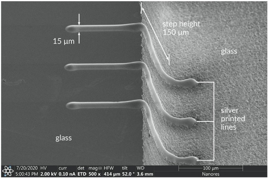 Repeatable and continuous silver lines with a width of 15µm are printed on the step with a height of 150µm
There is a clear market need for heterogeneous integration for high-performance flexible hybrid electronics that combine printed electronics and silicon technology. The challenge we face is the integration of flexible ultra-thin chips (UTCs) on flexible foils as they are too fragile for conventional bonding methods. In this regard, UTCs printed on the flexible PCB using XTPL’s microdispensing system show robust device performance under bending conditions, indicating the high reliability of both the chip thinning and bonding methods.
The ability to print such interconnectors using the UPD approach has been successfully demonstrated in the literature (see Ma, S., Kumaresan, Y., Dahiya, A. S., Dahiya, R., Ultra-Thin Chips with Printed Interconnects on Flexible Foils. Adv. Electron. Mater. 2022, 0, 2101029. https://doi.org/10.1002/aelm.202101029): to fabricate flexible ultra-thin MOSFET chip, thinned chip was attached to a flexible PCB and interconnections were printed between the chip and the PCB. This work demonstrated the ability of the UPD technology to connect fragile ultra-thin chips without damaging them, as well as the ability to print interconnections resistive to bending on flexible substrates.
Printing structures for high-frequency signals
Challenge: avoid high-frequency signal losses caused by poor geometrical homogeneity and structure integrity
Samples printed using UPD have unique features important for high-frequency applications: high surface smoothness, constant linewidth, and constant linespace, which limit signal losses. Therefore, UPD gains competitive advantages over other additive manufacturing technologies. Aerosol Jet Printing is limited to 20 µm gap size because of overspray. Moreover, the appearance of the satellite droplets around the printed signal line will produce radiation on the substrate.
XTPL’s UPD approach gives printed structures tailored for signals above 300 GHz. Apart from the interline gaps limitation, the common problems are the high roughness of deposited structures (limiting the transmission frequency) and low adhesion to the substrate. UPD deals with these issues: printed silver lines are smooth, and adhesion to a wide range of substrates is very high. The substrate types include glass, silicon, flexible foils, and RO4003.
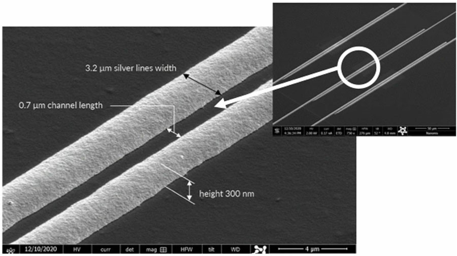 Example silver lines printed on a PEN foil. The line width is 3.2µm, and the interline distance is 0.7µm (a distant view of the sample is in the inset)
Printing flexible devices: sensors
Challenge: using both high and low viscosity materials within single printing method
The unique features of the UPD technique for biosensing applications include 1) deposition of both, high-viscosity and low-viscosity 3rd party materials (suitable for functional materials and bio-probes); 2) low-cost and disposable needles that are easy to change to avoid contamination between the various functionalisation steps (e.g., antibody/ethanolamine/BSA); 3) material cost reduction: deposition of micro-areas or micro-dots for matrix system fabrication (like ELISA plate) minimising the amount of bio-liquid required.
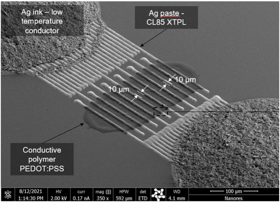 An example design for bio-sensing applications
The UPD approach answers the critical challenges in the fabrication of high-density microelectronics: high-resolution printing of various materials on complex substrates. The essential feature of UPD is the ability to print high-viscosity inks using nozzles with a diameter of the order of micrometres. It is possible to obtain structures with arbitrary shapes, including lines, dots, crosses, and meshes. The printed feature size is as small as 1 micrometre with electrical conductivity up to 45% of bulk value. UPD can become an indispensable tool for rapid prototyping and microfabrication thanks to these features.
Conclusions
The printing technology developed by XTPL enables an enabling approach for applications which cannot be done with already known subtractive methods and for use-cases, where other additive approaches cannot fulfil all the requirements. Together with strong industry partners, XTPL is in the technology scaling up process, providing solution compatibility with production automation and throughput requirements.
The unique approach introduced by XTPL is also available for R&D and prototyping centres (both industrial and academic) thanks to the Delta Printing System, which is commercially available since late 2020 and today has a rapidly growing global network of users. The current customers appreciate the extraordinary versatility of this technology, the adaptability of the printing system, and the outstanding customer support offered by XTPL.