


The SiC FET in a ‘cascode configuration comes closer to the ideal power switch, believes Dr Anup Bhalla, VP engineering at UnitedSiC
Wide bandgap semiconductors are being promoted as the future of power switching with their potential for higher speed and lower losses. Converter designs however, have to allow for some practical limitations that vary between the different devices on the market.
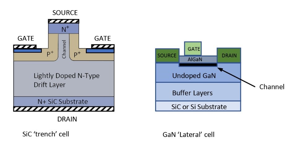
Figure 1: Comparison of SiC FET and GaN high electron mobility transistor (HEMT) cells
The basic feature that sets WBG materials apart from silicon (Si) is in the name. The energy required to move electrons from the atomic valence to conduction band, the band gap, is higher at 3.2eV for silicon carbide (SiC) and 3.4eV for gallium nitride (GaN) compared with just 1.1eV for Si. This translates to much higher electric field breakdown performance and higher peak temperatures before failure. SiC also has 3.5 times the thermal conductivity of Si. Together, these features allow high voltage and power levels, switched at high frequency and high temperature.
Wide bandgap choices
GaN discretes have yet to be adopted in volume, so looking at SiC, the preference is most often for MOSFET devices that are normally-off enhancement-mode. They do have some disadvantages however. One is that the MOSFET integral body diode has a high forward voltage drop and relatively high recovery charge which varies typically by a factor of three over temperature. This results in high losses in circuits that force the diode to conduct such as choppers, hard-switched bridges with inductive loads and PFC stages using the popular bridgeless totem pole arrangement. Using a parallel SiC Schottky diode adds cost and complexity with limited benefits.
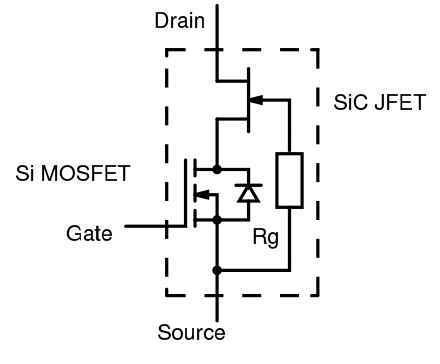 Figure 2: The SiC FET cascode arrangement
Another consideration is that SiC MOSFETs often have lower voltage threshold (Vth) values to allow for low RDS(ON) values. For most suppliers, the gate source voltage has to be kept within tight limits with not much margin between recommended operating voltages and maximum rated voltages, especially for negative voltage from gate source (VGS). SiC MOSFET Vth also suffers from hysteresis issues.
Finally, short-circuit saturation currents tend to be high at operating gate voltages, and can lead to device degradation in SiC MOSFETs especially for repetitive stress, a major concern for system reliability.
The SiC FET
The simple SiC JFET has no body diode or fragile gate oxide but is inconveniently normally-on with zero gate voltage and only off with around -7V gate source. Although they have their applications as circuit breakers, they are problematic in circuits that could have shoot through, such as bridges. One solution is to combine a SiC JFET with a low voltage Si-MOSFET in a cascode arrangement (Figure 2), known as a SiC FET.
When the MOSFET gate is positive, it turns on, shorting the JFET gate to source through Rg, turning it on. If the MOSFET gate is at 0V, it is off and its drain voltage rises to the point where the JFET gate is about -7V with respect to its source, turning it off. Dynamically, the MOSFET drain voltage stays at 12 to 20V due to the capacitive divider effect of the near-zero CDS of the JFET and the finite CDS/CGD of the MOSFET. This means that the MOSFET can be a low voltage type with correspondingly very low RDS(ON) of a few milliohms, usually 1/10 to 1/30 compared with the on-resistance of the JFET. The cascode now forms a normally-off high-voltage switch.
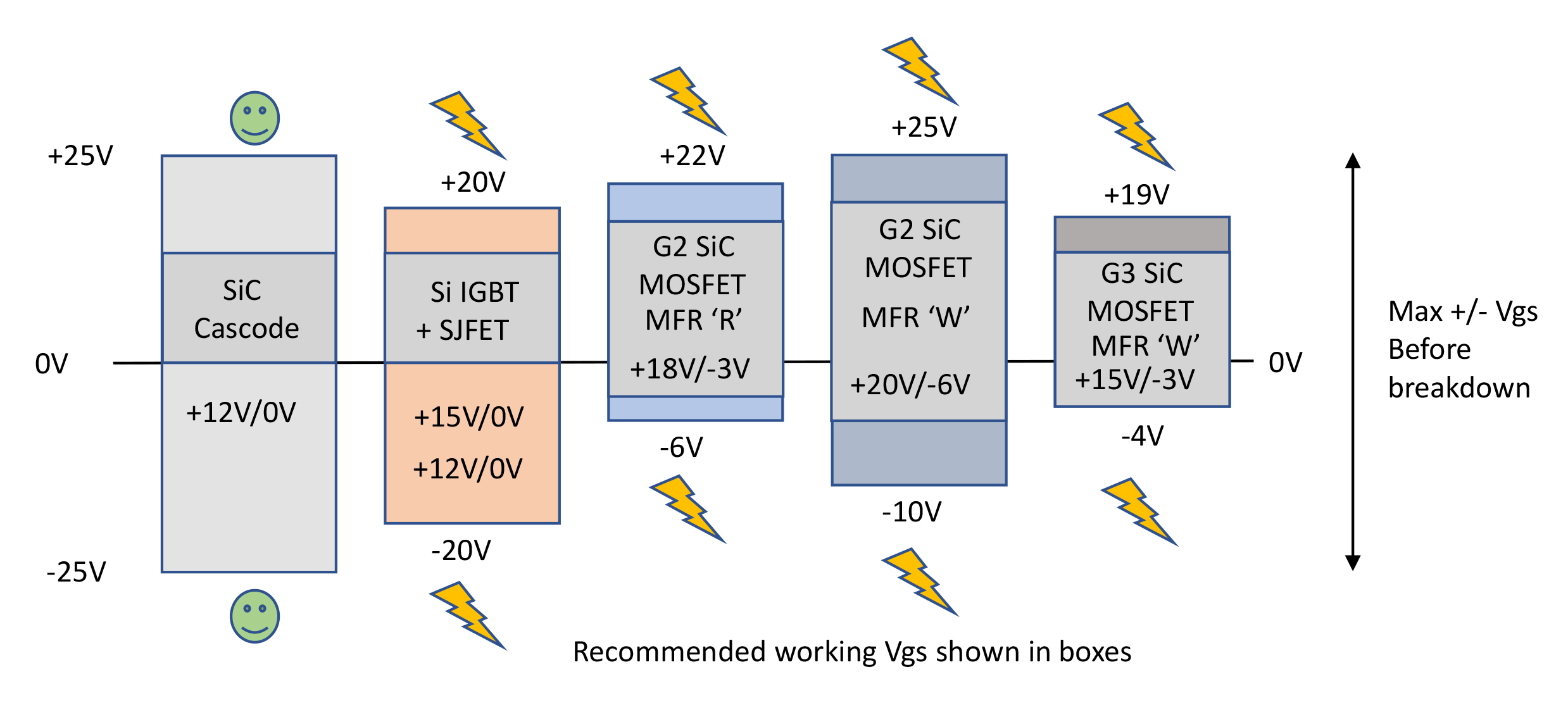 Figure 3: Comparison of gate drive voltage levels for IGBT, Si and SiC devices
The body diode of the specially designed MOSFET is a low voltage type. The recovery charge is very small and around 20 times less than a standard 600V fast recovery diode. An extra parallel diode is not therefore necessary in circuits that require a reverse conduction path.
Another benefit of this design is that gate drive voltage is now not critical, typically 0 to 12V with a maximum of ±25V allowable. Furthermore, short-circuit saturation current does not depend on gate voltage but only on the channel ‘pinch-off’ effect, which has a self-limiting, negative temperature co-efficient. The high temperature rating of SiC gives extra margin of safety.
The low-voltage MOSFET also has very low input capacitance, minimising gate drive power requirements, while the vertical geometry of the JFET results in near zero Miller capacitance, eliminating the possibility of dV/dt induced turn-on. Another benefit is that the cascode output capacitance is also very low, half the value or less, of a comparable voltage Si or SiC MOSFET, resulting in lower switching loss EOSS.
Due to their uncritical gate drive, SiC FET cascodes can often be dropped in to replace Si-MOSFETs or even IGBTs for an instant boost in performance with perhaps just gate resistor value changes to control edge rates. In contrast, SiC MOSFETs would require quite different gate drive circuits with more precise voltage drive levels (see Figure 3). With the SiC FET substituting for Si MOSFETs and IGBTs, snubbers can often be reduced in value and parallel diodes omitted for efficiency and cost savings. Mechanical compatibility is also maintained with SiC FETs available in the popular TO-247 and TO-220 packages.
If a system is designed around SiC FETs from the ground up, there are dramatic benefits to be had by increasing switching frequency while still improving efficiency for smaller and lower cost filter components and heatsinking.
Where to use SiC FET cascodes
SiC FET cascodes are available with 650 and 1200V ratings with RDS(ON) values less than 30mΩ and current ratings up to 85A. This makes them suitable for applications in industry such as motor drives, inverters and welding. In the bridge circuits typically used, voltages are clamped to the DC power rail as a maximum, so the 1200V devices can be used safely in 690V AC systems with the 650V parts in lower voltage single phase systems. A stack of multiple JFETs and a single Si-MOSFET, or super cascodes, result in switches rated up to 10kV.
Topologies that match the SiC FET capabilities are the phase shifted full bridge (PSFB), LLC, used above about 500W and the bridgeless totem pole PFC stage where the SiC FET fast body diodes allow fixed-frequency continuous conduction mode. This reduces peak currents and inductor size, increasing efficiency and easing EMI filtering provision.
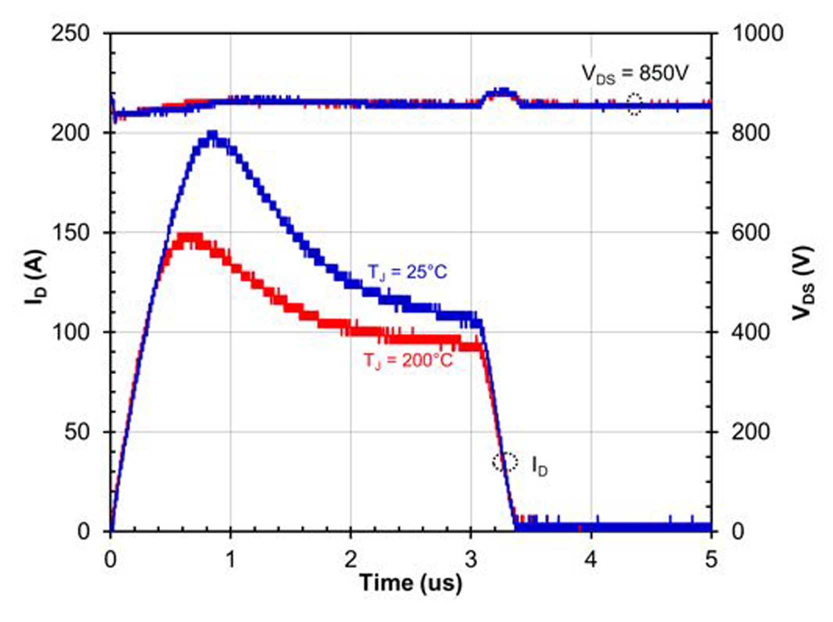 Figure 4: SiC FET short circuit current reduces with time and starting temperature
Although IGBTs are still commonly used in the automotive drivetrain, wide bandgap devices are the obvious choice for better efficiency, smaller size and lower weight. There are concerns about the reliability of the new technology for SiC MOSFETS with their limited and variable short-circuit withstand capability. SiC FETs however, have the proven ability to reliably meet the 5µs short-circuit specification, typical for automotive use. With their positive temperature co-efficient of RDS(ON), the devices also naturally reduce current over time and have lower peak currents from higher starting temperatures. The effect also ensures current flow is uniform across the die. Figure 4 shows results of testing at United SiC with a 1200V device.
To address over-voltage in automotive applications, SiC FETs have excellent avalanche rating; with a voltage transient, the internal JFET gate-drain junction breaks over, turning the channel on and clamping the voltage.
The future
Packaging innovations for SiC FETs allow more of the devices’ potential to be exploited. For example, three-terminal Kelvin connections in leaded packages eliminate source inductance effects making faster gate drive feasible. Stacking co-packaged JFET and Si-MOSFET is being introduced soon to lower cost and shorten interconnections. Bare die is being offered to assemble into modules for very high-power applications.
At low power, SiC FET die are even finding their way into auxiliary supplies and adapters where their efficiency and robustness is coupled with minimum unit component count.
PCIM Europe Visit UnitedSiC – Hall 9-432