


There are many reasons to use GaN-on-Si power transistors such as eGaN FETs, in telecoms, vehicles, healthcare and computing.
Figure 1 shows a comparison of eGaN FETs and Si MOSFETs. The normalised die size is on the vertical axis compared against rated device voltage, shown on the horizontal axis. The blue dotted line is the theoretical limit for silicon MOSFETs. The green line shows modern GaN-on-Si FETs compared with the blue dots for Si MOSFETs. It should be noted that 100 V eGaN FETs are four times smaller than the best 100V MOSFETs.
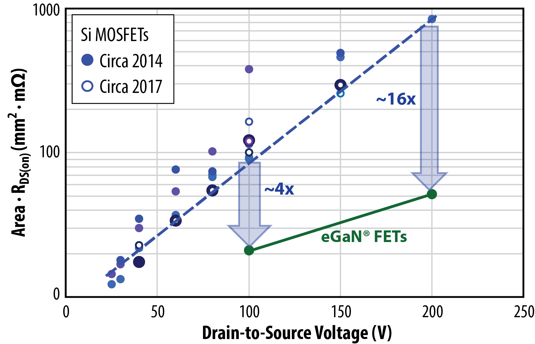
Figure 1: Comparison of sizes for GaN-on-Si FETs and Si MOSFETs
GaN is a superior semiconductor compared with Si. Devices made in GaN are smaller than the smallest possible Si MOSFETs and are also much faster than the fastest possible Si MOSFETs (see Figure 2). The switching figure of merit (FoM) is shown on the vertical axis compared with the rated voltage on the horizontal axis. The blue dotted line is the theoretical limit for silicon MOSFETs. The green line shows modern GaN-on-Si FETs compared with the blue dots for Si MOSFETs. The graph shows that 100V eGaN FETs are five times faster than the best 100V MOSFETs.
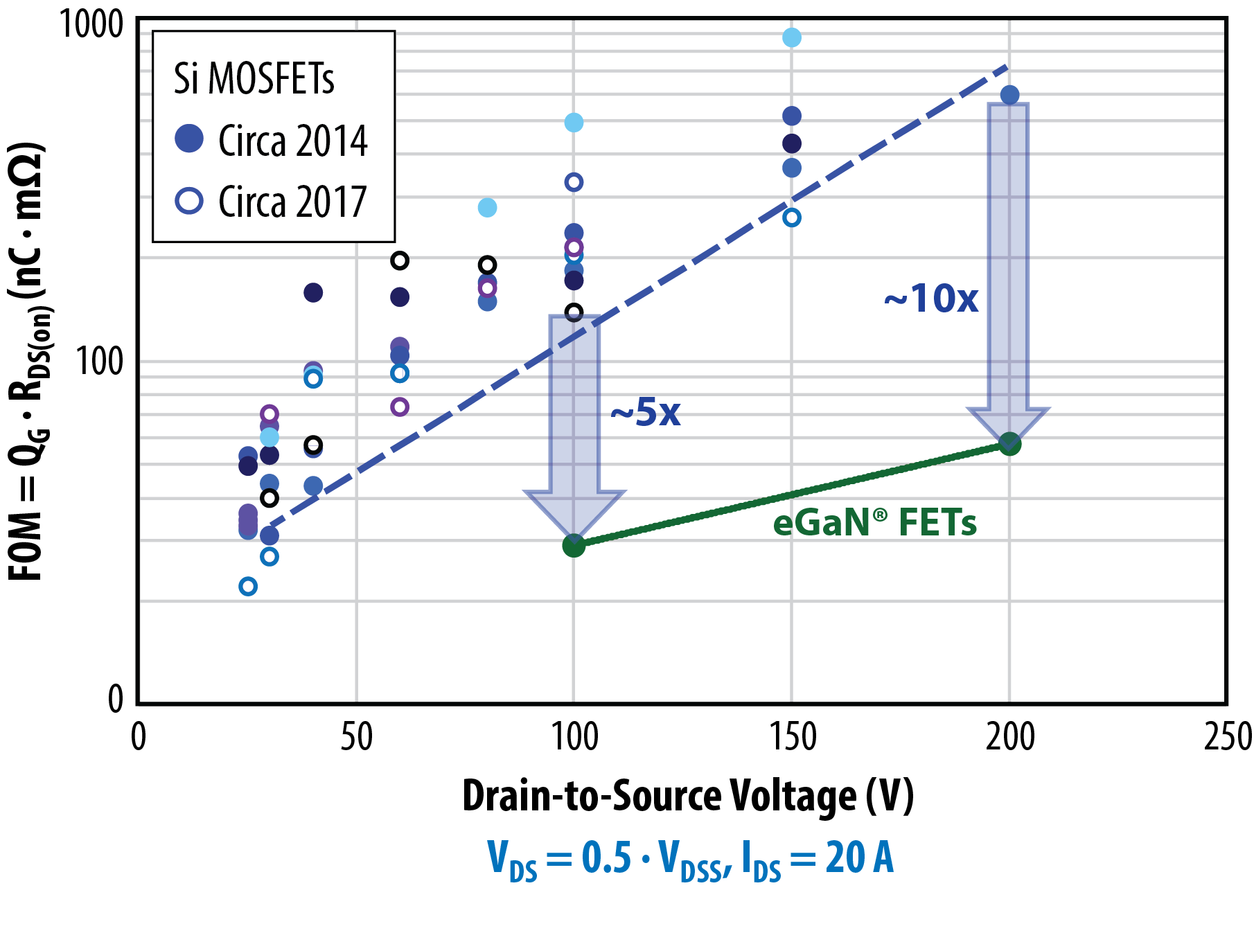 Figure 2: Comparison of GaN-on-Si FETs and Si MOSFETs switching
Automotive and medical use
For many applications that needed the speed or size, this was enough of a benefit to start buying large quantities. For example, the speed, range, and resolution of lidar systems used in autonomous vehicles is directly proportional to how fast you can drive a laser with a large amount of current. All the modern lidar systems designed for autonomous vehicles use eGaN FETs and ICs from Efficient Power Conversion (EPC) for these reasons.
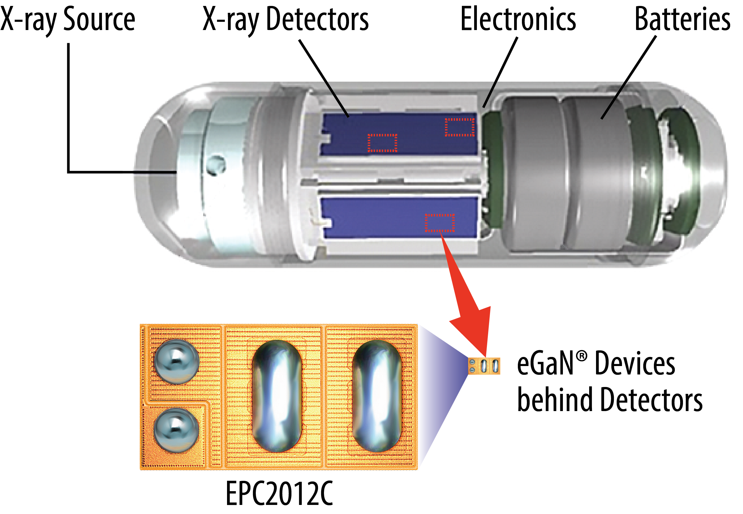
Figure 3: Check-Cap has developed an X-Ray machine that can be swallowed as a pill to create a high-resolution 3D image of a patient’s colon
In another example of early adoption of eGaN FETs (Figure 3) shows an X-ray machine that has been miniaturised to fit inside a pill that you can swallow. This pill, developed by the Israeli company Check-Cap and approved in EU countries, can perform a colonoscopy without requiring the patient to purge in advance of the procedure. The EPC2012C eGaN FET is used in the power section to efficiently generate high voltages in a tiny size. The patient takes the pill and wears a patch on his or her back for about three days as the pill journeys through the entire digestive system while wirelessly sending high-resolution images to the patch. This patch can then be sent into the doctor for interpretation, and the procedure is complete.
As production costs decreased and yields improved, the ability to compete on price with the aging Si MOSFET became possible. The first direct competition against MOSFETs started in late 2018 in a battle for 48V DC/DC power supplies. As shown in Figures 1 and 2, power supply designers realised that eGaN FETs could make higher power density and more efficient 48 V power supplies that are needed in high-density computing applications for cloud computing, artificial intelligence (AI), machine learning, and gaming applications. Record power density and efficiency could be realised with simple topologies such as the 900W DC/DC converter using an LLC topology shown in Figure 4. A power density of about 1700W/in3 (104W/cm3) is achieved with an overall efficiency above 98%.
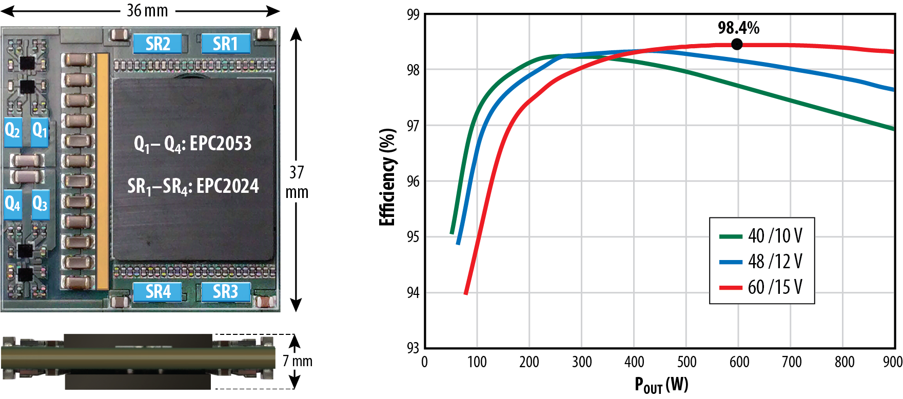 Figure 4: A 900 W DC/DC converter uses EPC2053 eGaN FETs on the nominal 48 V primary side and EPC2024 eGaN FETs on the nominal 12 V output secondary side at greater than 98% efficiency
New 48V DC/DC power supply designs are rapidly adopting eGaN FETs to reduce the size, increase efficiency, and lower cost considerably.
Automotive companies are beginning to adopt a 48V distribution bus in mild-hybrid cars. The reason for 48 V instead of the traditional 14 V bus is that electrical loads are increasing from a few hundred Watts at the turn of the century, to 2.5 – 8 kW in a modern mild-hybrid (also known as power-assist hybrids, battery-assisted hybrid vehicles or BAHVs). Wire harnesses become too stiff and bulky at 14V if they must efficiently convey hundreds of amperes of current. With a 48V bus handling the heavy loads and the 14V bus handling legacy loads such as infotainments and navigation systems, the wiring harnesses become manageable and efficient. The requirements from these automotive manufacturers are for 48 to 14V converters that are bi-directional. They must also be highly efficient, reliable, and cost-effective. eGaN FETs designed into several of these systems will appear on cars in the next two to three years.
This is just the beginning for GaN. Even the latest devices on the market are about 300 times larger than they could be if we could make them at the theoretical limits for GaN. For perspective, Si MOSFETs were 300 times larger than they are now when they were first introduced in the late 1970s. GaN will get there, and in so doing will continue to widen the performance and cost gap compared with Si MOSFETs.
GaN power ICs
GaN-on-Si power FETs have been in production at EPC for 10 years, with millions of devices used in envelope tracking for telecomms basestations, lidar for autonomous vehicles and robots, implanted medical devices, truck headlamps, satellites and DC/DC power supplies for computers, servers, gaming systems, and advanced artificial intelligence (AI) systems.
The company has been producing GaN power ICs since 2014. The first devices were monolithic half bridges for power supplies and motor drives. The integration saves space, reduces circuit inductance and therefore boosts efficiency and reduces cost. The next step was to add drivers and level shifting functions to achieve a full power stage on a single GaN-on-Si chip (Figure 5).
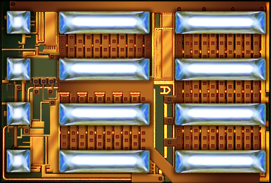 Figure 5: The EPC2151 GaN IC is in beta testing and is set to launch in early 2020
The EPC2151 IC has drivers and level shifting integrated into a single chip with the two 100V enhancement-mode transistors in a half-bridge configuration. It measures 3.9 x 2.6mm and conducts 10A at 1MHz with 48VIN and 12VOUT.
The goal is to drive towards complete systems on a single GaN-on-Si chip where the user supplies a logic level input to result in high-performance power conversion.
Smaller, faster, lower cost, and more integrated, GaN-on-Si devices have spent a decade gaining the confidence and trust of designers across the spectrum of power conversion applications. In the second decade, we expect most new designs to favour GaN-on-Si devices over solutions with aging power MOSFETs. We expect discrete solutions to remain most of our demand for the next two years, after that, ICs should begin to dominate. Silicon is starting to fade, followed by discrete transistors. The winner is the power conversion consumer.