


A recent Electronic Specifier webinar, hosted by Paige West, Managing Editor, brought together leading experts from the power electronics industry to discuss the evolving landscape of wide bandgap semiconductor technologies, focusing on gallium nitride (GaN) and silicon carbide (SiC).
The panel included Laszlo Balogh, DMTS, High Voltage Power, Texas Instruments, Pietro Scalia, Head of System Architecture and Marketing for Power, Renesas Electronics, Kamal Varadarajan, PhD, Director of Technology Development, Power Integrations, and Dr. Peter Friedrichs, Fellow SiC at Infineon Technologies.
The session aimed to provide practical insights into the characteristics, applications, and future directions of GaN and SiC, which are increasingly critical in power electronics due to their superior power density, efficiency, and thermal performance.
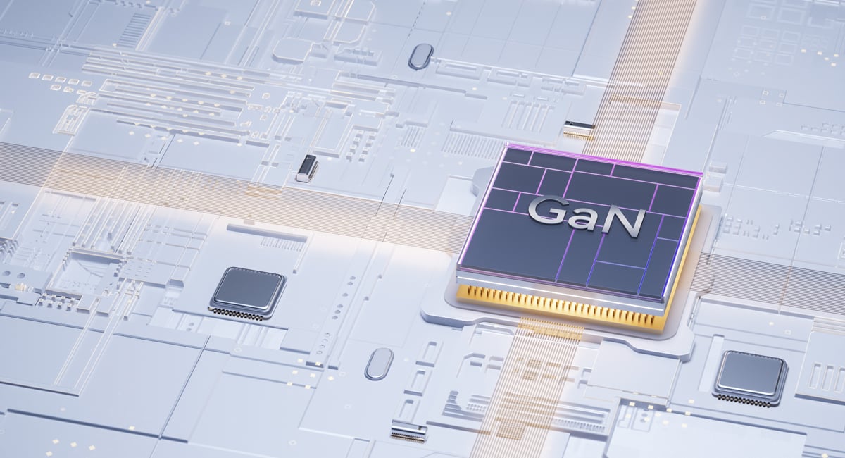
The discussion began with an overview of what makes GaN and SiC ‘wide bandgap’ semiconductors. Scalia explained that the key differentiator is the bandgap energy, with both materials offering significantly higher values than traditional silicon. This results in higher critical electric fields and greater robustness. GaN excels in electron mobility, enabling faster switching speeds, while SiC stands out for its superior thermal conductivity, making it ideal for high-power, high-temperature applications.
The panellists agreed that these fundamental material properties dictate where each technology is best applied.
Dr. Friedrichs elaborated on the structural differences between GaN and SiC devices. GaN is predominantly a lateral device, which allows for easier integration and the creation of advanced circuit topologies, such as bidirectional switches. SiC, on the other hand, is typically a vertical, bulk-based device, more akin to traditional silicon MOSFETs and IGBTs. This structural distinction influences system design choices, with GaN favoured for high-frequency, compact applications and SiC for high-voltage, high-power scenarios.
The conversation then shifted to specific applications. Balogh highlighted that GaN is commonly used in fast chargers for consumer electronics due to its efficiency at lower power levels, while SiC is preferred for automotive powertrains and industrial drives where higher voltages and power are required. The panellists emphasised that the choice between GaN and SiC is highly application-dependent, with each material offering unique advantages.
A significant portion of the webinar addressed the balance of efficiency, cost, and reliability in system design. Varadarajan noted that both GaN and SiC have achieved high levels of reliability, with established JEDEC standards and extensive qualification testing. He stressed the importance of integration in maximising the benefits of wide bandgap devices, particularly as efficiency improvements become incremental. Integration enables precise control and further miniaturisation, which are essential for extracting the last percentages of efficiency.
Scalia and Dr. Friedrichs discussed the evolving market landscape. GaN, initially adopted in consumer applications, is now penetrating automotive and industrial markets, thanks to its versatility and the development of higher voltage devices. SiC remains dominant in high-power, high-voltage applications but faces increasing competition as GaN technology advances. Both panellists agreed that system-level considerations, such as topology and magnetics, play a crucial role in technology selection.
The panel also explored manufacturing strategies and supply chain considerations. Renesas and Infineon are investing in larger wafer sizes (200mm and 300mm, respectively) to drive down costs and increase production volumes. This shift is expected to bring GaN and SiC closer to cost parity with silicon, further accelerating adoption. The panellists highlighted the importance of owning the manufacturing process, particularly for GaN, where process control is critical to device performance and reliability.
Reliability and quality were recurring themes. Varadarajan detailed the rigorous testing protocols used to qualify GaN and SiC devices, including high-temperature, high-voltage, and humidity stress tests. He emphasised that modern wide bandgap devices exhibit excellent field reliability, with failure rates well below industry thresholds. Scalia added that understanding the specific failure mechanisms of each technology is essential, and that ongoing standardisation efforts are helping to mature the industry.
During the Q&A session, the panel addressed audience questions on topics such as the complementarity of GaN and SiC, leakage currents, device structure, and the role of integrated device manufacturers (IDMs) versus foundries.
Watch the webinar on-demand below: