The Large Hadron Collider (LHC) presents a tough case for electronics. Situated inside a 17-mile long tunnel that runs in a circle under the border between Switzerland and France, the LHC is a massive scientific instrument that accelerates particles close to the speed of light before smashing them together. The collisions yield tiny maelstroms of particles and energy that hint at answers to questions about the building blocks of matter.
These collisions also produce an enormous amount of data – as well as enough radiation to scramble the bits and logic inside almost any piece of electronic equipment.
This is a challenge to CERNs physicists as they attempt to probe deeper into the mysteries of the Higgs boson and other fundamental particles. Off-the-shelf components can’t survive the harsh conditions inside of the accelerator and the market for radiation-resistant circuits is too small is to entice investment from commercial chip manufacturers.
“Industry just couldn’t justify the effort, so academia had to step in,” said Peter Kinget, the Bernard J. Lechner Professor of Electrical Engineering at Columbia Engineering. “The next progress made by ATLAS will be triggered by one Columbia chip and measured by another.”
Kinget leads the team that designed specialised silicon chips that collect data in one of the harshest and most important environments in particle physics. Their most recent paper outlining the project was published on 1st July in the IEEE Open Journal of the Solid-State Circuits Society.
“These sorts of collaborations between physicists and engineers are very important to advancing our ability to explore fundamental questions about the universe,” said John Parsons, professor of physics at Columbia University and leader of the Columbia team working on the ATLAS detector, one of the LHC’s massive instruments. “Developing state-of-the-art instrumentation is crucial to our success.”
Radiation-resistant circuits
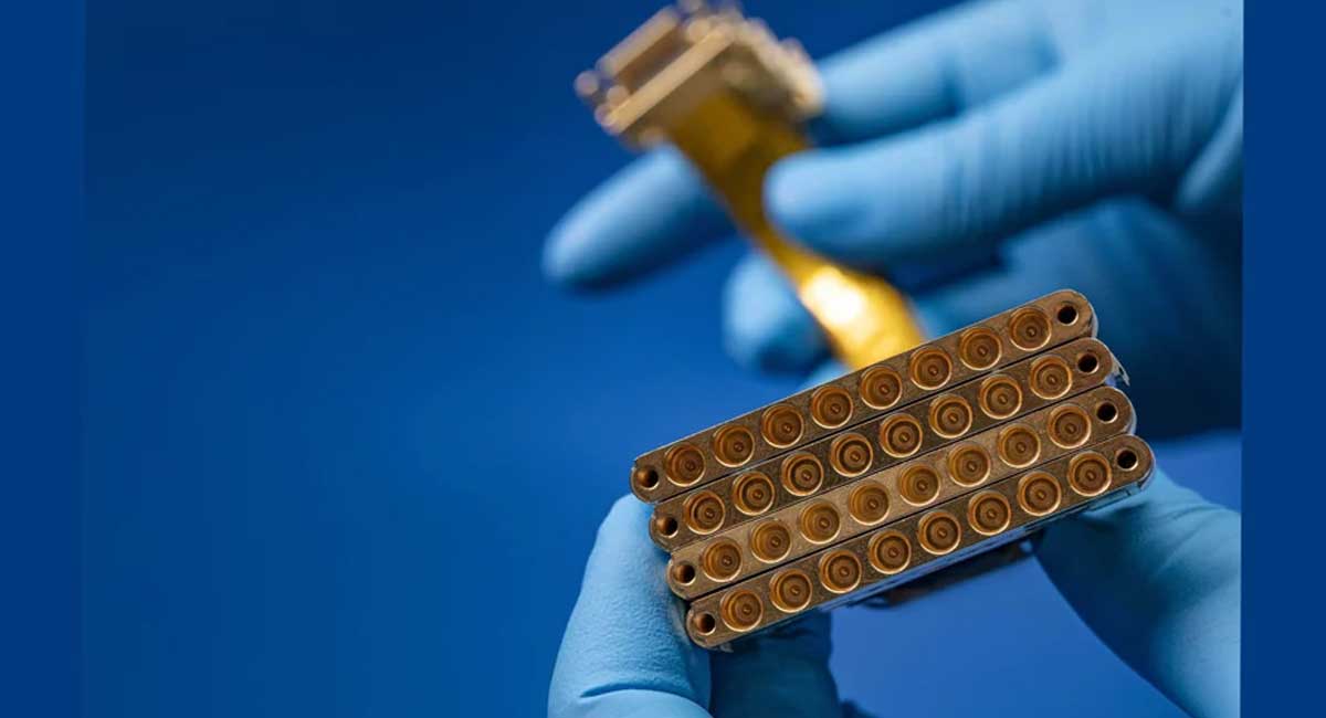
The devices the team designed are analog-to-digital converters (ADCs). Their task is capturing electrical signals produced by particle collisions inside of CERN’s detectors and translating them into digital data researchers can analyse.
In the ATLAS detector, the electrical pulses generated by particle collisions are measured utilising a device called a liquid argon calorimeter. This enormous vat of ultra-cold argon captures an electronic trace of every particle that passes through. Columbia’s ADC chips convert these delicate analog signals into precise digital measurements, capturing details that no existing component could reliably record.
“We tested standard, commercial components, and they just died. The radiation was too intense,” explained Rui (Ray) Xu, a Columbia Engineering PhD student who has worked on the project since he was an undergraduate at the University of Texas. “We realised that if we wanted something that worked, we’d have to design it ourselves.”
Rather than creating entirely new manufacturing methods, the team used commercial semiconductor processes validated by CERN for radiation resistance and applied innovative circuit-level techniques. They carefully picked and sized components and arranged circuit architectures and layouts to minimise radiation damage, and built digital systems that automatically detect and correct errors in real time.
The resulting design is resilient enough to withstand the especially challenging conditions at LHC for more than a decade.
Two Columbia-designed ADC chips are anticipated to be integrated into the ATLAS experiment’s upgraded electronics. The first, called the trigger ADC, is already operating at CERN. This chip, initially described in 2017 and validated in 2022, allows the trigger system to filter about a billion collisions each second and to instantly select only the most scientifically promising events to record. It serves as a digital gatekeeper deciding what merits deeper investigation.
The second chip, the data acquisition ADC, recently passed its final tests and is now in full production. The chip, which was described in an IEEE paper earlier this year, will be installed as part of the next LHC upgrade. It will very precisely digitise the selected signals, enabling physicists to explore phenomena like the Higgs boson, whose discovery at CERN made headlines in 2012 and led to the Nobel Prize in physics in 2013, but whose exact properties still hold mysteries.
Both chips represent the kind of direct partnership between fundamental physicists and engineers.
“The opportunity as an engineer to contribute so directly to fundamental science, is what makes this project special,” added X.
It further created opportunities to collaborate across multiple institutions. The chips were designed by electrical engineers at Columbia and at the University of Texas, Austin, in close collaboration with physicists at Columbia’s Nevis Laboratories and the University of Texas, Austin.