


Fabricated using Toshiba’s new CMOS5 65nm process, the TC320 ASIC family combines a low-k dielectric with up to eight levels of copper and one level of aluminium interconnect. Analogue and application-specific digital IP cores can be mixed on the same chip, while memory options include embedded DRAM (eDRAM), tightly stacked semi-embedded DRAM, and single- and multi-port SRAM.
Toshiba’s new technology offers double the logic density of its previous generation 90nm process, a 30% reduction in power per gate and a 20% reduction in gate delay. A multi-threshold technique allows mixing of logic cells operating at different logic voltages while core voltages down to just 1.2V coupled with advanced power saving techniques reduce dynamic power consumption and leakage current.
The TC320 family offers synthesis-friendly primitive cells designed to address high speed and low power requirements. Two types of I/O cells support requirements for high pin count and core limited designs respectively. A wide range of mixed-signal and digital IP cores include ADCs, DACs, ARM and MIPS processors and options for Ethernet, HDMI, ATA, PCI and USB connectivity.
Toshiba is supporting the new TC320 technology with advanced design environment that will significantly reduce turn-around-time (TAT). Toshiba’s European LSI Design & Engineering Centre (ELDEC) can also help to minimise TAT through dedicated project management and support for every stage of the SoC and SiP design and implementation process.
Discussing the launch of the TC320 technology, Eugen Pfumfel, a Principal Engineer for SoC market and application development at Toshiba, states: “High-quality multimedia streaming and gaming applications are pushing integration levels, memory size and speed requirements to the limit. At the same time there is a need to widen the interface to external components through high speed serial links and double data rate parallel interfaces. Toshiba’s TC320 technology supports these design requirements, while our combination of advanced design methodologies and local support dramatically shortens development time for European customers.”
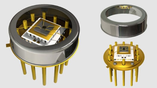
TC320 designs can be supplied in a variety of packaging options that meet the requirements of advanced SiPs. For designs requiring high pin counts (600 to over 2000), flip-chip BGA packaging (PBGA[FC]) offers high I/O density and electrical performance, while PFBGAs with 41 to more than 300 balls pins are optimal for applications requiring minimal form factor. PBGAs with 256 to 868 pins are cost-effective solutions for mid-range I/O pin count requirements. For price-sensitive applications with low pin-count, the extremely thin WCSP (Wafer Level Chip Scale Package) is available. QFN options are also available.