


Parasitic inductance is a factor in motor inverter applications. By reducing the amount of parasitic inductance, power dissipation during turn on is reduced. In addition, the high side drive reliability is improved due to limiting negative voltage spikes in the drive voltage, VS (Figure 1).
Figure 1: Parasitic inductance between IGBT emitter and gate driver
In motor inverter applications where a low side power switch or IGBT is connected to the gate driver via a current sensing, parasitic inductance components between the power IGBT emitter and gate driver should be understood. The total parasitic inductance is composed of the emitter wire bonding, PCB pattern trace, and inductance of the shunt resistor as shown in Figure 1. The high current transition (dic/dt) that occurs during low side turn on results in energy loss (Eon) and a large negative VS spike voltage due to this additional parasitic inductance. VS is the gate driver control voltage. VS is connected to high side IGBT emitter (Figure 1). VS is essentially a floating ground that is referenced by the upper IGBT in the half bridge configuration.These values (Eon, negative VS spike) increase with the amount of power that is switched. Higher power motor inverters applications are even more susceptible to the resulting power loss and voltage spiking from parasitic inductances.
Voltage drop
Parasitic inductance between the IGBT emitter and gate driver generates a gate drive voltage drop during turn on. During this time, the IGBT gate-emitter voltage VGE is reduced by an amount of (VDD – Vdrop) as shown in the equation below.
- c/dt) x ( parasitic L)
Where Vdrop = VL1 + VL2 from Figure 2
The gate-to-emitter voltage during time t1 is decreased by the parasitic inductance voltage drop. This additional voltage across the parasitic inductance increases the turn on energy Eon. In the system the gate resistor is used to control the gate timing intervals. During turn on the dic/dt slope is proportional to the IGBT collector current. Similarly, the gate-emitter voltage drop is increased in proportion as collector current increases. To prevent increase of the Eon energy loss to the parasitic L and voltage spiking, a low inductance shunt resistor is recommended.

Figure 2: Power IGBT turn on timing diagram, current path and G-E voltage drop
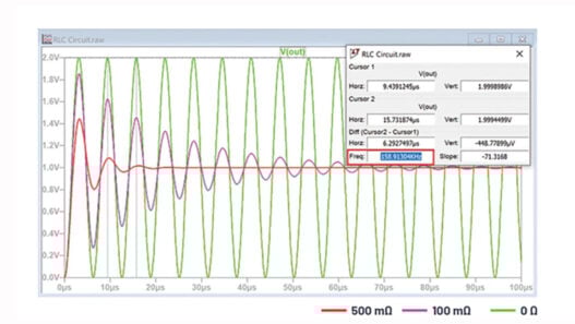
Figures 2 and 3 show examples of comparison by using two kinds of shunt resistors with two 1200V IGBT configured like Figure 1 (it can be half-bridge configured power modules or discrete IGBTs). One shunt resistor has a larger parasitic inductance (L=50nH) than the other (6nH). This results in additional energy losses of up to 33% from 4,500 to 6000uJ respectively.

Figure 3: Turn on energy EON increases with collector current based on the amount of parasitic inductance present in the shunt resistor
In addition to energy loss, larger parasitic inductance value can potentially stress or damage on high side driver (HVIC) in motor inverter applications. In the case of a HVIC solution, there is limitation for allowable negative VS spike voltage. This limitation is called the VS negative pulse safe operating area (VS-NPSOA).
The parasitic inductance of shunt resistor causes a negative VS spike voltage due to the dic/dt current transition of the low side freewheeling diode current when the high side IGBT turns off. The larger 50nH inductance increases the negative VS spike. The result is a voltage spike of -41.3V. This is an increase from -31.1V or 33% when compared to the 6nH value of parasitic inductance.
Efficiency tactics
It is recommended that a low inductance shunt resistor be used for better efficiency and stable operation in inductive load applications. Using a shunt resistor with a lower parasitic inductance will reduce energy losses up to 33% while ensuring operation within the safe operating area of the gate drive voltage source.
Motor Control design tool that can help new or experienced motor control and motor drive engineers evaluate and design with power modules rather than discrete solutions in minutes. It provides switching and conduction losses over the input data range, and accepts sine PWM, space vector PWM, and four discontinuous PWM methods. Other features are ΔTj (ripple temperature) at a specified motor frequency and a predictor of module’s long term reliability. A graphical display shows junction temperature ripple for low inverter output frequency, and heatsink thermal requirements to meet the given criteria are provided. The design tool calculated losses using equations and empirical results.
PCIM 2015: Hall 9 – 342