


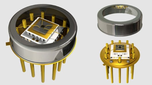
The 20nm 8 gigabyte (GB) NAND device from Intel and Micron delivers the highest capacity in the smallest form factor. Manufactured by IM Flash Technologies, the NAND flash joint venture from Intel and Micron, the new device is a breakthrough in NAND process and technology design, further extending the companies’ lithography leadership.
Shrinking NAND lithography to this technology node is the most cost-effective method for increasing NAND output to date, providing approximately 50 percent more gigabyte capacity than current technology. The new 20nm process technology also helps further the companies’ dual goal to enable instant, affordable access to the world’s information.
The growth in storage all the way from the data center to full-featured smartphones and tablets is creating new demands for NAND flash technology, especially greater capacity in smaller designs, said Glen Hawk, vice president of Micron’s NAND Solutions Group. Micron is proud of the industry-leading technology we have developed with Intel, and we’re pleased to have this technology honored by the Flash Memory Summit.
NAND silicon process and die level innovation is foundational for the flash memory industry to provide compelling end solutions like solid-state drives, said Tom Rampone, Intel vice president and general manager of the Intel Non-Volatile Memory Solutions Group. We are pleased that the Flash Memory Summit continues to recognize the innovation and success that Intel and Micron are achieving together.
Additionally, the new 20nm 8GB device measures just 118mm2 and enables a 30 to 40 percent reduction in board space (depending on package type) compared to existing 25nm 8GB NAND devices. A reduction in the flash storage layout provides greater system level efficiency as it enables tablet and smartphone manufacturers to use the extra space for end-product improvements such as a bigger battery, larger screen or adding another chip to handle new features.
Flash Memory Summit is the only conference dedicated entirely to flash memory and its applications. It is intended for system designers, analysts, hardware and software engineers, product marketing and marketing communications specialists, and engineering and marketing managers. It features forums, half-day tutorials, paper and panel sessions, and expert tables. Subjects include harsh environments, laptops, enterprise storage system applications, consumer products, performance, product design, caching methods, design methods, software, new technologies, market research, testing and reliability, and security. The Summit also includes exhibits of the latest products and product awards.