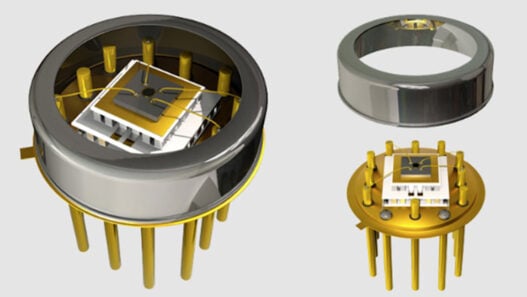
The proprietary AllGaN half-bridge GaN Power IC with iDrive monolithically integrates functions required to deliver switching speeds of up to 2MHz and enable a dramatic reduction in size, cost and weight while delivering faster charging, claims the company.
Half-bridge circuits are used in smartphone chargers and laptop adapters, as well as TVs, solar panels, data centres and electric vehicles (EVs). According to the company, older silicon-based half-bridge components have slow switching and parasitic power losses, which slows speeds by up to a factor of 30.
The first half-bridge GaN Power IC available from the company is the 650V-rated NV6250. It is offered in a 6.0 x 8.0mm QFN complete with dual drivers, level shifter, dual 560mOhm power FETs, bootstrap circuit and protection features. Simple, low-power digital PWM inputs switch the half-bridge at all frequencies. It is compatible with a range of analogue and digital controllers from multiple IC partners.
The company has been working with partners to create the next generation of adapters and chargers.
Samples and demonstration boards for the NV6250 are available immediately to qualified customers, with production planned for Q2, 2017.


