


More specifically, he will discuss and critically benchmark Laser Direct Structuring (LDS), aerosol, 3D Printed Electronics (3DPE), two-shot molding and In-Mold Electronics (IME).
This article is based on the newly updated report ‘In-Mold Electronics 2020-2030: Technology, Market Forecasts, Players‘ which offers a detailed assessment of various techniques to obtain 3D-shaped circuits with a special focus on IME.
This report from the global market research firm, offers a technical assessment of manufacturing processes and material requirements, market outlook for applications and players, and a study of competitive routes to 3D electronics.
What drives these trends?
Interconnects are often created in Printed Circuit Boards (PCB). These PCBs can be made on flexible substrates, mainly PI, enabling the realisation of thin, flexible, multilayer circuits. PI has a relatively high processing temperature which means that it is compatible with standard reflow processes. As such, the assembly process is similar to that found on common PCBs, e.g. FR4 based rigid PCBs. Furthermore, multilayer circuits can be achieved. As such, complex high density circuits supporting all manners of IC packages can be realised.
These flexible circuits can be fitted into tight areas and/or around non-flat surfaces. However, they are neither very flexible nor truly conformable. As such, they limit design freedom. Furthermore, they take additional space and will require extra assembly steps.
Consequently, there is a need to create interconnects on arbitrary-shaped 3D objects to overcome these shortcomings. These techniques have enabled many applications ranging from antennas to wearable devices to automotive and white goods parts.
Approaches: No one-sizes-fits-all
1) LDS (laser direct structuring)
LDS or laser direct structuring is, by now, a well-established technology. Here, a laser scans a pattern on a special plastic substrate which contains embedded conductive metal or metal oxide additives.
The scan rate is typically around 4m/s whilst the typical linewidth is 150-200um although a focused laser can be implemented to achieve much narrower linewidths, e.g., 60um or so. The laser removes the surface in the scanned areas, exposing conductive parts which are then Cu plated and thus metallised. The change of design is digital and thus requires no additional tool.
The process has some shortcomings, namely that (a) the object volume is restricted (typical work volume is around 400x70x80 mm3), (b) it works on already metallized surfaces, (c) it requires special polymers, (d) the pick-and-place, where needed, and the associated adhesive dispensing will need to take place on 3D objects, (e) the production step up can occupy a relatively large real estate due to the plating equipment, and (f) the lines may not be sufficiently thick to support power (vs signal) functions (note: lines are typically less than 20um thick and electroplated at 5-8um/hr rate. Galvanic plating can boost rates to 1um/min).
Nonetheless, this technology already had success, especially in mobile phone antennas. These antennas were directly deposited on the plastic part, enabling 3D design and eliminating the extra FPCB. The challenge is that the antenna designs in phones are evolving, especially for 5G mobiles, likely forcing this technology out.
Furthermore, this technology failed to break into other markets in a serious way. Of course, many applications were demonstrated, and multiple are manufactured in relatively small volumes. But none is large enough to compensate for the competitive pressures present in the antenna business.
The equipment supply market had, in particular, been in freefall given that there was sufficient installed capacity to service the existing and short term foreseeable demand and given that suppliers had increased despite the original developers seeking to enforce their claimed IP rights.
2) Aerosol
Aerosol deposition was a direct competitor to LDS. It too offers a way to metallize already 3D-shaped objects. It, too, allows digital control of the pattern, thus enabling rapid turnarounds and viability even for small production runs. The built volume here is, like LDS, small.
The process is different from LDS. Here, a high velocity jet of particle mists is formed and directed at the object for metallization. This high velocity jet, e.g., more than 50m/s, remains highly collimated, giving rise to narrow linewidth capability, e.g., 10-20um for laboratory machines. The machine thus consists of one or multiple aerosol jet heads, which are maneuvered in 3D space using robotic arms, and curing unit(s). Therefore, the process has a very small physical footprint.
The mist is composed of particles, mainly nano-sized Ag particles, e.g., 50-150nm or so in diameter. These inks will need to exhibit high particle size monodispersity or else they will create a gradient in the jet, resulting in non-uniformity. Furthermore, the inks will need to show good adhesion across a range of common plastic substrates, e.g. PC or PC/ABS blends.
They will also need to achieve high conductivity at increasingly low curing temperatures. A rate-limiting step will be the curing time, thus rapid cure formulations are desirable. Despite this, it is claimed that the TACT is shorter than LDS. Since the conductive traces are formed out of inks, they are not as conductive as plated copper.
This technology also found success in antenna production. The installed base is around 16-18 production-level machines or so. Some of the early generations of products however reached their end of life. It remains to be seen whether there can be new waves of antenna or similar applications opportunities for aerosol in the coming years. This will be the challenge that defines the future of aerosol 3D metallization.
3) 3D Printed Electronics
3D printing is a major market already. It is used in prototyping and increasingly also in production. The materials menu covers plastics, metals as well as ceramics.
The plastic 3D printed objects often only fulfil a mechanical role. As such, we can consider them ‘dumb’ structures. Therefore, the ability to integrate electronics into the 3D object would enable designers to 3D print ‘intelligent’ objects.
To achieve this, the electronic components must be mounted on or within the 3D object. If they are to be mounted on the outer surface, then the pick-and-place and assembly can take place after the completion of 3D printing. If they are to be placed within the object, then the two processes must be coupled, and the assembly must take place as part of the 3D printing process.
In all cases, the components will require interconnections. This would be for signal as well as power transmission. To get the best out of the possibilities offered by 3D printing, these interconnections would need to be embedded inside the structure (not just the outer surface) and would need to cover a 3D space (not just metallizing a 2D plane within the 3D object).
Achieving this opens many new product design possibilities. It will have a low production speed; however it can offer design and product customisation opportunities. Multiple companies and entities are pursuing various strategies to enable this.
In particular, some are trying to streamline the software design process and to create a library of plug-and-play compatible electronic parts. Finally, note that some are using conductive plastics as the 3D printing feedstock. These additive-loaded filaments however, have sufficient conductivity for applications such as electrostatic discharge and are unlikely to be good enough for circuity.
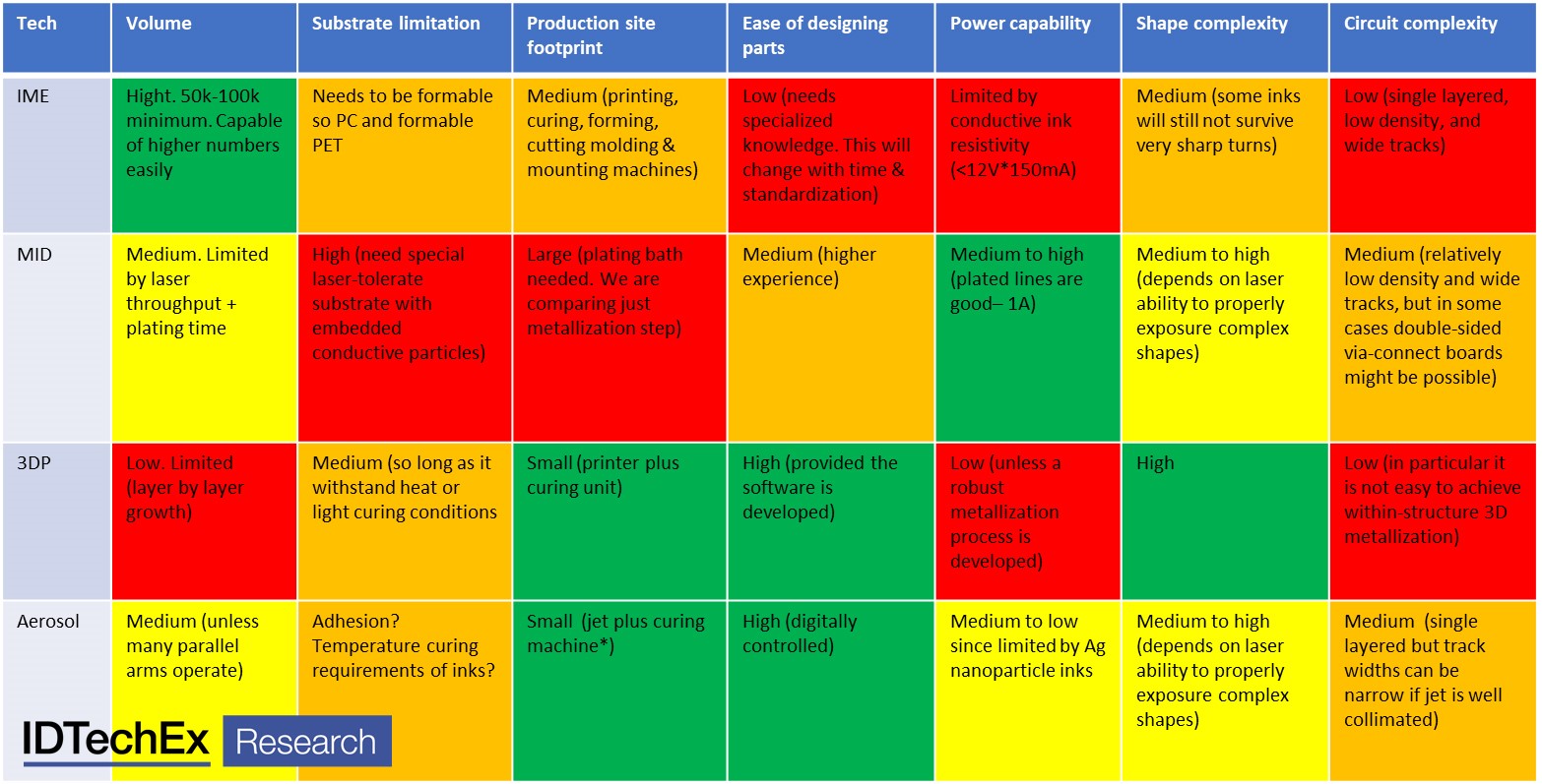
4) Two-Shot Molding
Another technique is two-shot molding. Here, two resin types are employed with one containing conductive catalyst (Fe or more commonly Pd) and the other being catalyst-free. The two parts are molded over each other such as only the to-be-plated parts of the catalyst-containing resin are exposed.
The 3D-shaped molded part is then put through roughening, cleaning, plating, and finishing to create the final 3D-shaped metallized part. There are applications for this, including some insulin pumps.
5) In-Mold Electronics
In-Mold Electronics (IME) is another route to create 3D-shaped metallized parts eliminating the use of additional PCBs. Here, the functional and graphic inks are printed on one or two flat films, e.g., PC, and the rigid ICs pick-and-placed. This flat, functional sheet can then be 3D formed before being injection molded.
This technology, which in some ways is an evolution of in-mold decoration, is indeed very well-differentiated from those outlined above. The production rate and the product sizes can be higher and larger here, respectively. The pick-and-place can occur on 2D surfaces, easing and speeding up the process.
The process can therefore be more productive, leading to lower per-unit costs. As such, this technology can target very different markets. Furthermore, the electronics are truly structurally integrated, meaning that the aesthetic and outer graphics of the part can be preserved. Finally, other features such as light guides can also be structurally integrated.
Many innovations have been required to bring the technology to this step including (a) stretchable conductive inks, (b) special adhesives formulated to withstand the process conditions, and (c) thin optical guides to spread light. Furthermore, process know-how development is absolutely vital.
This technology also has some challenges, all which represent material innovation and process optimisation opportunities: (a) reliability needs to be very high as the embedded nature of the electronics eliminates post-deployment repair opportunities, (b) the conductive lines are signal carrying given their low conductivity, (c) the design is not straightforward given that many material and process materials must be considered and thus still represents an art, (d) the production has a steep learning curve and there is little modularisation yet.
Nonetheless, this technology is, in IDTechEx’s assessment, on the path to success, despite some previous setbacks, e.g. Ford product recall. IDTechEx forecast that this market can exceed $1bn by 2029 despite the slow take-off.
This success will come in smaller simpler steps first, meaning the first generation of products will be relatively small volume with low circuit complex and relaxer reliability requirements. Automotive applications to arrive from 2022-2023 onwards in notable volumes.
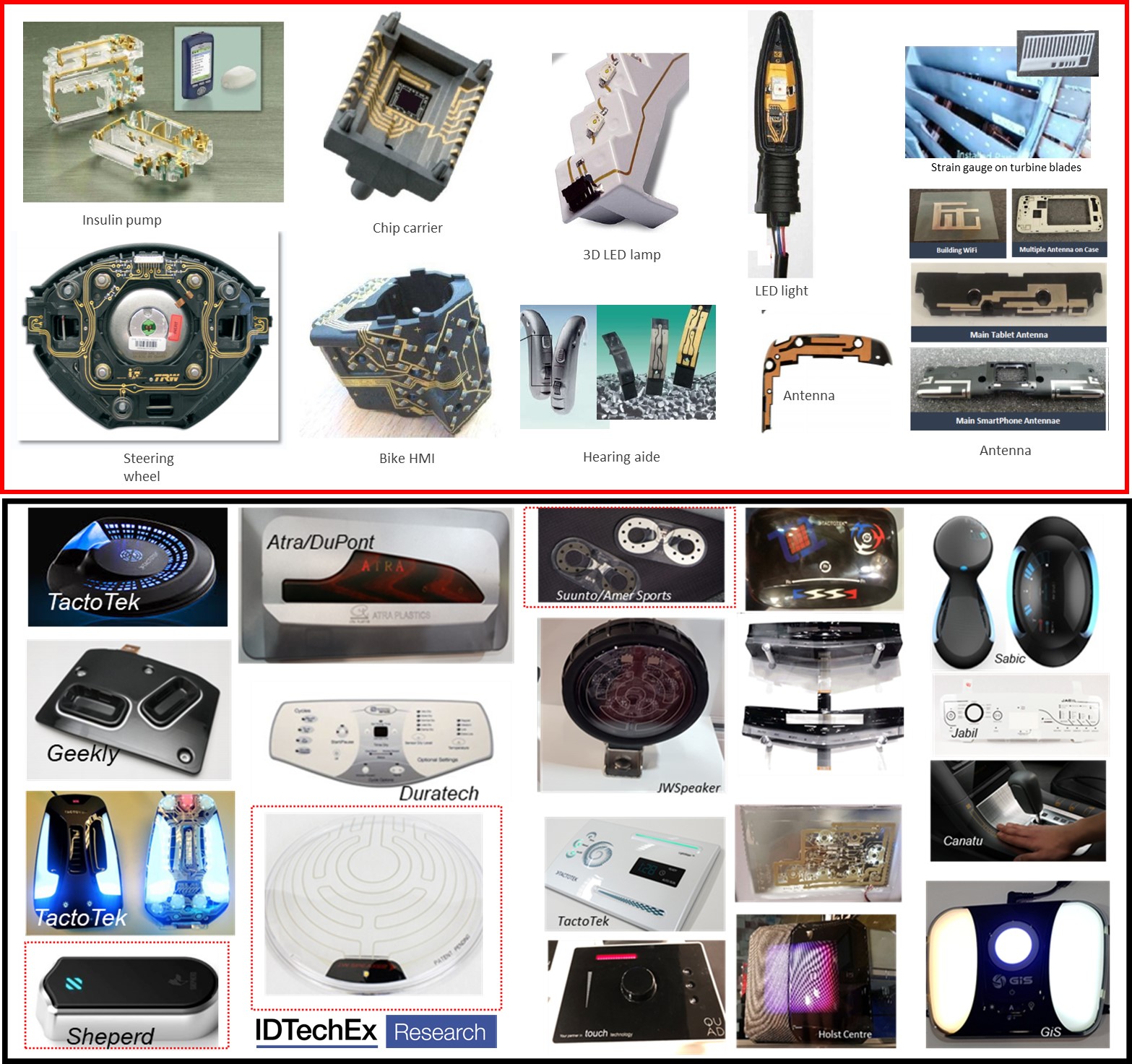
The panel in red shows product examples using two-shot molding, LDS, and aerosol. The bottom panel shows products and prototypes for IME. Sources are various including but not limited to Insulet, Zollner, SelectConnect Technologies, BMW, Kromberg & Schubert, GE, Lite-On, Atra, TactoTek, Geekly, JWSpeaker, Jabil, GiS, etc.