


Miniscule features over complex systems require higher precision, while greater throughput is often needed to meet market needs. Laser control and precision motion systems have been crucial in overcoming these challenges and advancing PCB production, particularly in techniques such as stencil manufacturing and laser direct imaging (LDI).
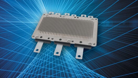
PCB stencil manufacturing
PCB stencils are made of stainless steel, and feature laser-cut openings that control the amount of solder paste applied to the pads. As electronic devices have advanced, these openings have become smaller, requiring mechanical systems with tighter synchronisation of motion and laser control. Furthermore, the X-Y plane is no longer sufficient, as ‘multi-level’ stencils need a Z-plane to create voids to optimise solder paste control or correct coplanarity problems. To this end, gantry motion systems now need to provide two or three linear degrees of freedom – X-Y or X-Y-Z – as well as offering the long travels and high speeds to meet the demands of modern PCB stencil manufacturing.
Unfortunately, there is the possibility of errors when mechanical acceleration limits are exceeded, but slowing down the process is often not an option. Advanced motion controllers – such as ACS-based A-824 and G-900 with EtherCAT® connectivity by Physik Instrumente (PI) – have largely overcome this challenge by providing ‘look ahead’ intelligence that automatically reduces laser speed where errors may exceed specification, which is especially common in sharp cornering. ‘Sky writing’ is another option for optimising corner quality, as it eliminates abrupt changes in velocity or sudden stops that increase time and cause errors. The ability to adjust laser power and pulse placement – as well as the capacity to turn it on and off – is also vital, requiring communication between the motion controller and the laser, which can easily be achieved, for example, using PI’s Laser Control Module.
Laser Direct Imaging
LDI is another technique increasingly used to create PCBs, owing to its precision and ability to produce smaller feature sizes. LDI uses a laser to directly build the circuit on the board, eliminating the need for the photo tools used in traditional imaging processes that can cause distortion or degradation. However, this method requires extremely high precision over the X-Y plane to ensure straightness and minimal yaw errors. High performance ACS motion controllers again provide the necessary performance, with excellent capabilities for extremely tight synchronisation between the laser and the positioning stages.
These technologies are not only helping manufacturers keep up with the incessant demand for PCBs, but they also deliver the levels of precision needed with ever-tightening design specifications.
PI in brief
PI (Physik Instrumente), headquartered in Karlsruhe, is the market and technology leader for high precision positioning technology and piezo applications in the semiconductor industry, life sciences, photonics, and in industrial automation. In close cooperation with customers from all over the world and for 50 years now, PI’s specialists (approx. 1,300) have, again and again, been pushing the boundaries of what is technically possible and developing customized solutions from scratch. More than 350 granted and pending patents underline the company’s claim to its leadership. PI has six production sites and 15 sales and service offices in Europe, North America, and Asia.