


By Andy Cai, Applications Manager, COMSOL
To be honest, I understand where the hesitancy is coming from. It’s true that simulation can’t fully replicate real-world conditions. There are some environmental and operating conditions and failures that software programmers or users cannot predict or measure and therefore can’t input. However, simulation is not about creating perfect models or getting perfect results; it’s about making better decisions earlier in the product development process, where informed decisions are most crucial. Achieving this requires looking at results that mimic real-world conditions as closely as possible and being able to easily iterate, and this is where simulation comes in. While not perfect, simulation – multiphysics simulation, in particular – is highly accurate when configured and used appropriately.
When integrated into daily design work, as opposed to being treated as a one-off report, simulation can transform how we understand and solve problems. We are living in a nonlinear world, and we have to take a multiphysics approach to study it. In this article, we’ll first discuss the advantages of multiphysics couplings in general, and then we’ll dive into specific uses within semiconductor packaging.
The case for coupling
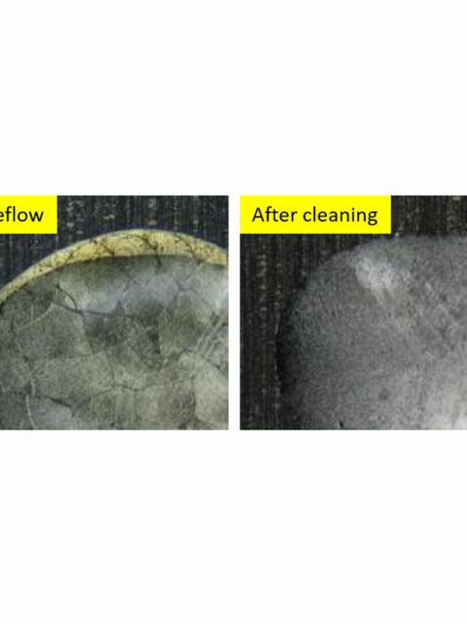
Multiphysics interactions in real-world materials and devices are inevitable, and modeling all of these effects leads to more accurate simulation results. For instance, heat causes expansion, expansion changes geometry, geometry changes affect impedance, and so on, and unless your simulation connects these dots itself, your design might be missing something critical. As a result, you might miss important information about your work. To give an example, we have seen customers use simulation to study residual stress in solder joints after reflow. The thermal model looked fine, and the stress model looked fine, but it wasn’t until the two models were coupled that the warpage started to match what was on the board. It wasn’t magic; the simulation was just finally accounting for how heat and mechanics really work together, in a deformed configuration.
As another example, what once seemed like a signal integrity issue turned out to be tied to slight geometric deformation during thermal cycling. This issue wouldn’t have been caught without coupling the structural and electrical sides of the physics equations.
Compared to traditional design methods, multiphysics simulation offers a more accurate and precise view of complex interactions in semiconductor devices, including interactions between heat, stress, electricity, and fluids. Moreover, simulation complements testing. Simulation can’t replace testing, but by performing virtual tests initially and prototyping an optimised design rather than multiple early-stage designs, the testing stage can require less physical iteration and required resources.
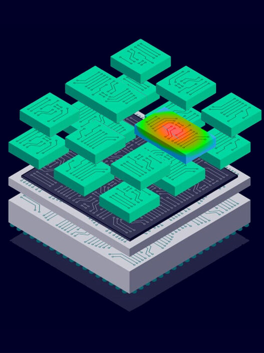
Where multiphysics really moves the needle in semiconductor packaging
Multiphysics simulation has made a difference in various areas of packaging. Below, I highlight some of these application areas.
Process simulation
Wet and dry etching processes are critical when creating features in semiconductor packaging. With wet etching, we’re dealing with chemical reactions and mass transport and are aiming for controlled etch depth with specific profiles. The right tools will let you model the interaction between fluid transport, diffusion, and reaction kinetics in order to optimise etch uniformity. Figure 1 shows a modeling example that examines how copper substrate material is depleted and how the cavity shape evolves during the wet etching process. This modeling is particularly important for the patterning of an integrated circuit.

Figure 1. A 2D model example showing wet chemical etching with laminar flow.
In soldering, the reflow process introduces thermal gradients, phase changes, and mechanical stress. We can simulate how solder balls melt and solidify and how nonlinear material behaviours like creep and plasticity affect joint integrity over multiple thermal cycles. Multiphysics makes it possible to capture metallurgical transitions that change material properties and residual stress states, which is essential for predicting reliability.
When it comes to underfill and encapsulant materials, we’re looking at complex non-Newtonian fluid behaviour, rheological models, and temperature-dependent properties. As these materials cure, they undergo volume shrinkage, creating residual stress and warpage. Simulating both the chemical kinetics and the resulting mechanical deformation in the same model offers a complete picture of assembly behaviour.
Mechanical reliability
Environmental factors like humidity and moisture diffusion can lead to swelling, vapor pressure increases, and delamination, fatigue, and cracking. Modelling how stress interacts with temperature and moisture can help you predict mechanical reliability. To give an example, simulation has been used in the industry for preconditioning projects involving temperature cycling and moisture soak, and when vapor pressure buildup and hygroscopic swelling were modelled together with mechanical deformation, the failure locations matched the test results almost exactly.
Figure 2 shows a model of the preconditioning process of a surface-mount device (SMD). The simulation results show the stress that occurs due to temperature and humidity, and these results can be used to evaluate potential damage and, if needed, help determine design changes before performing reliability testing on the end product.
Figure 2. A model showing the preconditioning process of an insulated-gate bipolar transistor (IGBT) module.
For mechanical reliability, we need to account for shock, vibration, and static loads. Semiconductor packages must withstand various dynamic stresses in mobile or automotive environments. A multiphysics approach can be used to evaluate package response to base excitation or sudden mechanical loads as well as static stresses from bending, torsion, or compression during handling and operation.
Thermal management
Today’s chips run hot, and passive cooling doesn’t always cut it. In the design of chips and systems that use thermoelectric coolers (TECs) and fans, coupled thermal–fluid models make it possible to virtually optimise the systems and avoid thermal bottlenecks that might occur with physical prototypes.
Nowadays, simulation tools make it possible to include all three heat transfer mechanisms – conduction, convection, and radiation – in a single model. Additionally, some thermal sources come from electromagnetic loss mechanisms like ohmic losses or eddy currents. By coupling electromagnetic and thermal physics, we can simulate phenomena like Joule heating in interconnects or localised hotspots in shielded regions.
Additionally, it is possible to model complete thermal control loops with a TEC connected between a chip and a heat sink. A model can couple thermal conduction in solids, nonisothermal airflow across fins, and a PID control algorithm that dynamically adjusts the TEC power. This kind of integrated approach makes it easy to evaluate not just passive dissipation but also active temperature control within operating ranges.
Electrical performance
Warpage and stress can shift trace geometry, which messes with impedance and signal speed. With the right model, you can simulate how thermal expansion alters signal paths and ESD or EMI behaviour. You can extract equivalent RLC matrices, simulate signal propagation with skinning and proximity effects, and evaluate how geometry and materials affect transmission line behaviour. These capabilities can help when assessing impedance matching, insertion loss, and crosstalk before fabrication.
By importing layout files directly from ECAD tools, you can also perform full electromagnetic analysis on actual routing and layer stack-ups, bridging the gap between layout and physical modelling. These simulations predict radiated emissions, immunity to external fields, and vulnerability to electrostatic discharge.
Validating simulation results with benchmarking
As mentioned earlier, there is still hesitancy toward adopting simulation in packaging, whether it’s because it seems difficult to validate simulation results or because sometimes simulation doesn’t match real-world results. This mistrust is why benchmarking matters, especially when you’re beginning to integrate simulation into established workflows. Compare the results against analytical results or experimental data as you build complexity. Also, don’t model everything at once. Instead, start with dominant effects and use submodeling, such as by creating a coarse global model and refining detail in critical zones only. This method keeps models manageable while still capturing key behaviour.
Benchmarking can also be improved by encouraging cross-disciplinary collaboration. Historically, different teams have owned different pieces of a project: Thermal engineers handle thermal elements, mechanical engineers handle mechanical components, and electrical sits in their own silo. This arrangement works – until it doesn’t. Accounting for various physics areas makes it possible to look at the bigger picture, and this often necessitates gathering data or getting help from simulation experts with difference specialities. Although you will still see electrical, thermal, and mechanical teams working independently, that’s slowly changing, and for the better. When different teams talk, simulation gets a lot more useful.
Looking to the future
The benefits of multiphysics couplings make simulation valuable within semiconductor manufacturing, and the capabilities and value of simulation tools are continuing to grow. What’s especially exciting is how simulation tools have recently been integrating machine learning to unlock new possibilities. For instance, with the COMSOL Multiphysics software it is possible to build surrogate models from simulation and measured data, and these machine learning models help to reverse-engineer the ‘black box’ behaviour in real-world packaging, especially when phenomena are hard to measure or model directly. This bridges simulation and factory data, enabling you to connect design, validation, and production feedback in one continuous loop. This is where the future of simulation is heading in the industry.
Final thoughts
Multiphysics isn’t a buzzword; it’s how the real-world works. Semiconductor packages are only getting more complex, and if we want to design with confidence, we need simulations that reflect that complexity. I’ve seen how multiphysics simulation can help teams catch problems early, avoid costly iterations, and explore more design options with less risk. Whether you’re running simulations yourself or making decisions based on them, simulation tools can lead to improved R&D in semiconductor manufacturing.