


By Daniel Murphy, Director of Technical Marketing, Cambridge GaN Devices
Until 2017, the power module used silicon IGBT technology, which is cheap but inefficient at low loads which is where a vehicle operates most of the time. Since the arrival of the Tesla Model 3, power modules using silicon carbide (SiC) switches have often been preferred because of the extra efficiency the wide bandgap technology brings. However, SiC is expensive to manufacture, therefore SiC power modules can cost more than twice that of IGBT versions. Now, a new solution is being developed using another wide bandgap material, gallium nitride (GaN) which promises to deliver high efficiency and low cost.
Silicon carbide technology has delivered tremendous benefits in terms of range and power, as power modules using SiC switches are around 5% more efficient in 400V bus vehicles more than IBGT modules (as per WLTP cycle). This translates into increased vehicle range and performance, or smaller battery size. The reduced switching losses of the wide bandgap technology are especially significant at lower loads of up to around 30%, where an EV inverter is operating most of the time. Small city run arounds will likely operate at higher load levels, but still, efficiency under 30% load is critical. This is why SiC is so beneficial, and tremendous strides have been made to develop the technology.
However, SiC MOSFETs remain expensive. Although devices achieved early commercial traction and have reached a level of production maturity, SiC manufacturing throughput is slower and far more energy-intensive to produce per unit area than traditional silicon devices, or, indeed, the other often-discussed wide bandgap material, gallium nitride. Therefore, the price of SiC devices is unlikely to significantly fall from current levels. In order to minimise the cost impact of SiC, a combinational approach has been proposed by several manufactures, which employs both SiC and IGBT switches in the same power module. With this approach, the SiC devices are used at lower loads and IGBTs operate together with the SiC at higher load levels. Efficiency is not as high as modules that are full-fit SiC, but still, gains of 3-4% can be realised.
Whilst this appears to be a reasonable compromise, the costs of the SiC element remain an issue. To address this, another approach using GaN has recently been proposed by Cambridge GaN Devices (CGD). GaN offers wide-bandgap technology benefits like SiC, so similar or even better power module and EV performance, range, and size advantages can potentially be achieved. GaN HEMTs currently cost more than their SiC counterparts, however, that is changing rapidly. GaN devices can be made on standard silicon fabrication lines using much of the same equipment and processing. Therefore, a clear pathway to cost reduction can be foreseen.
Crucially, unlike SiC, there are lower energy costs and the price of GaN is largely dependent on economies of scale. As more and more capacity comes onstream, and with the announcement of 8″ GaN fabs, the price of GaN HEMTs is dropping and we can expect crossover in price with SiC by 2028, with GaN set to fall even lower in the future, potentially to the same levels as IGBTs.
CGD has patented a combinational power module solution – Combo ICeGaN – which combines the company’s ICeGaN gallium nitride transistors with IGBTs from another vendor, resulting in a power module which will enable EV manufacturers to take advantage of the efficiency of wide bandgap switching together with low cost IGBTs giving an excellent cost performance trade off.
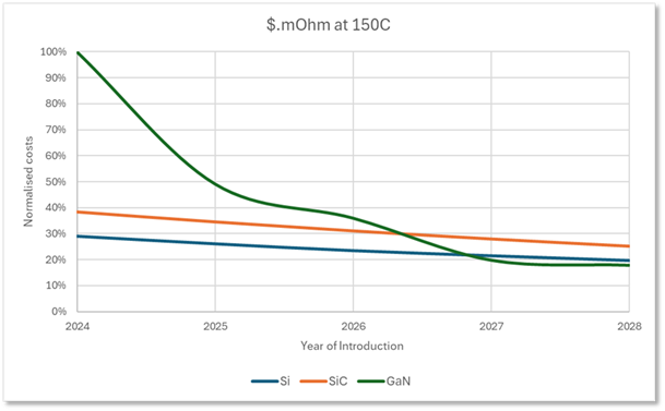
Figure 1: normalised price projection of SiC, GaN, and Si
CGD’s ICeGaN technology addresses the challenges that have previously prevented GaN’s adoption by the automotive industry. Firstly, the ICeGaN interface is monolithically integrated onto the same die as the GaN HEMT switch. The ICeGaN interface has circuit elements which make using the GaN HEMT easy – using only a standard silicon MOSFET driver. Secondly, ICeGaN has been proven to have excellent gate robustness. There are however some technical considerations to be addressed with GaN technology. GaN has a lower junction temperature (150°C) than IGBTs or SiC (both 175°C). CGD is addressing this with on-chip temperature sensing – with SiC, such sensing is more complex with a thermistor on the base plate attached via a wire bond. This on chip sensing allows far more accurate dimensioning and sizing of the GaN within the power module.
Secondly, the temperature coefficient of SiC is lower than that of GaN, meaning it has better relative performance at higher temperatures. However, in newer processing nodes, the temperature coefficient of GaN is improving significantly, and it can be expected that it will eventually approach that of SiC.
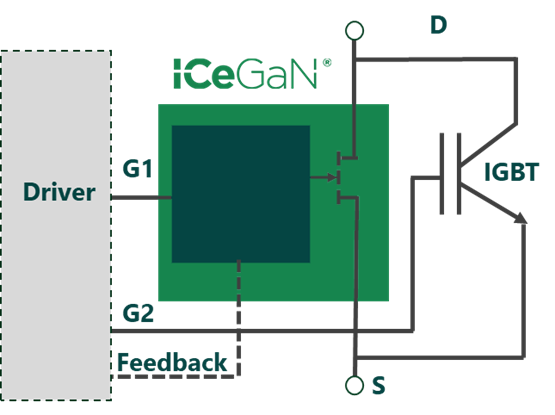
Figure 2: schematic representation of Combo ICeGaN
GaN – and ICeGaN in particular – has another major advantage. Unlike SiC, GaN is a lateral technology so other functions can be integrated on chip. ICeGaN already integrates the driver interface, Miller clamp and protection circuitry on the same die as the switch. In future, further integration (such as sensing) can be considered.
The proprietary Combo ICeGaN approach uses the fact that ICeGaN and IGBT devices can be operated in a parallel architecture having similar drive voltage ranges (e.g., 0-20V), as well as excellent gate robustness. As discussed earlier, the ICeGaN switch is very efficient with low switching losses at relatively low currents (light load), while the IGBT is dominant at relatively high currents (towards full load or during surge conditions). Combo ICeGaN also benefits from the high saturation currents and the avalanche clamping capability of IGBTs. At higher temperatures, the bipolar component of the IGBT will start to conduct at lower on-state voltages, supplementing the loss of current in the ICeGaN. Conversely, at lower temperatures, ICeGaN will take more current. Sensing and protection functions are intelligently managed to optimally drive the Combo ICeGaN and enhance the Safe Operating Area (SOA) of both ICeGaN and IGBT devices.
Figure 3 shows a schematic representation of a 3 phase inverter used in motor control (traction inverter) applications, employing Combo ICeGaN.
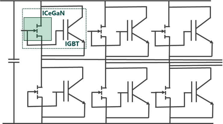
Figure 3: 3 phase inverter employing Combo ICeGaN
The power loss and efficiency curves for a standard IGBT power module and the Combo ICeGaN solution are shown in Figure 4. Overall, the combined solution will generate efficiency increases of around 3-4%. So, when in the near future, GaN drops lower in price than SiC, the Combo ICeGaN approach will offer the best price/efficiency performance. Eventually, as GaN approaches parity with IGBTs, then a GaN-only full-fit module using ICeGaN may well be the preferred option, and leading car makers are already investigating that.
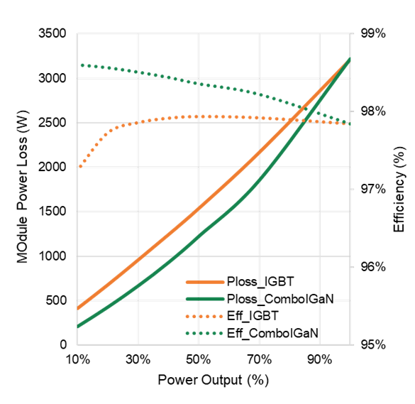
Figure 4: comparing power loss and efficiency across the load for IGBTs and Combo ICeGaN
This article originally appeared in the May’25 magazine issue of Electronic Specifier Design – see ES’s Magazine Archives for more featured publications.