


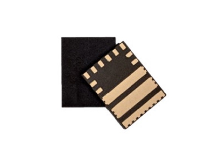
The ISG3201 is a complete half-bridge circuit that includes two 100V 3.2mΩ InnoGaN HEMTs and the required driver circuitry in an LGA package measuring just 5.0×6.5×1.1mm in size, making it both effective and compact.
Explains Yi Sun, General Manager of Innoscience America and Senior VP: “Innoscience is now offering designers a choice between the ultimate flexibility of using a discrete solution, and this new integrated approach which is very compact and simple to use and soldering and simplifying the power stage layout”.
The ISG3201 SolidGaN half-bridge comprises two 100V 3.2mΩ e-mode GaN HEMTs with driver, driving resistor, bootstrap and Vcc capacitors. It has a 34A continuous current capability, zero reverse recovery charge and ultra-low on resistance making it quite versatile. Thanks to the high level of integration, gate loop and power loop parasitics are kept below 1nH. As a result, voltage spikes on switching nodes are minimised. The Turn-On speed of the half-bridge GaN HEMTs can be adjusted using a single resistor making is customisable to specific needs.
ISG3201 is suitable for high frequency Buck converters, half-bridge or full-bridge converters, Class D audio amplifiers, LLC converters, and power modules. Overall, the integrated ISG3201 solution can save up to 20% PCB space on discrete GaN designs and 73% board space on traditional silicon implementations.
Adds Dr Pengju Kong, VP of Product Design Engineering at Innoscience: “The ISG3201 half-bridge device is the first in a whole family of SolidGaN integrated GaN-based solutions that Innoscience plans to launch this year, including further half-bridge circuits with different voltage ratings. Innoscience aims to offer engineers exactly what they want – integrated solutions or discrete devices – enabling them to achieve the best possible result for their design, minimising development time and reducing cost.”