


Data centres are hot right now – and not in a good way. The eruption in artificial intelligence has completely changed the energy demands of computing infrastructure.
Training and running AI models mean that massive amounts of data now need quick and constant movement; ergo, the memory systems that handle that work are now at a bottleneck. The more data that comes, the more power is consumed; therefore, more heat is produced, and so more cooling is required. It is a problem that will only compound as the world’s appetite for the surface gratification these systems offer grows. So how can materials help move innovation forward whilst making sure everything keeps its cool?
Silicon has been a kingpin in the semiconductor industry for decades, but nowadays, engineers are having to work hard to stretch the limits of what is possible to get every last ounce of performance gains from it. Whether that’s through architectural tricks like stacking chips in three dimensions or redesigning packaging. But these workarounds, though clever, have their limitations – so why don’t they look for improvements to the material itself? One of the reasons could be that silicon is such an abundant, versatile, and scalable material and, as the saying goes, if it ain’t (technically) broke, then don’t fix it.
Yet, there are rumblings that a smarter arrangement of silicon may not be enough, and that the answer may lie in a different material altogether. And many of those rumblings are looking towards graphene.
So, what can graphene do for us that silicon can’t? Graphene is a single layer of carbon atoms arranged in a hexagonal lattice. It’s been called a “wonder material” and a “material of the future” for years. Its isolation was awarded the Nobel Prize in Physics in 2010! It conducts electricity faster than silicon, dissipates heat efficiently, and is atomically thin. However, turning those properties into manufacturable electronic devices has been tricky, to say the least. But Cambridgeshire-based company, Paragraf, believes it has found a way to change that.
A semiconductor-compatible process
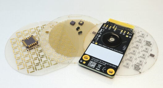
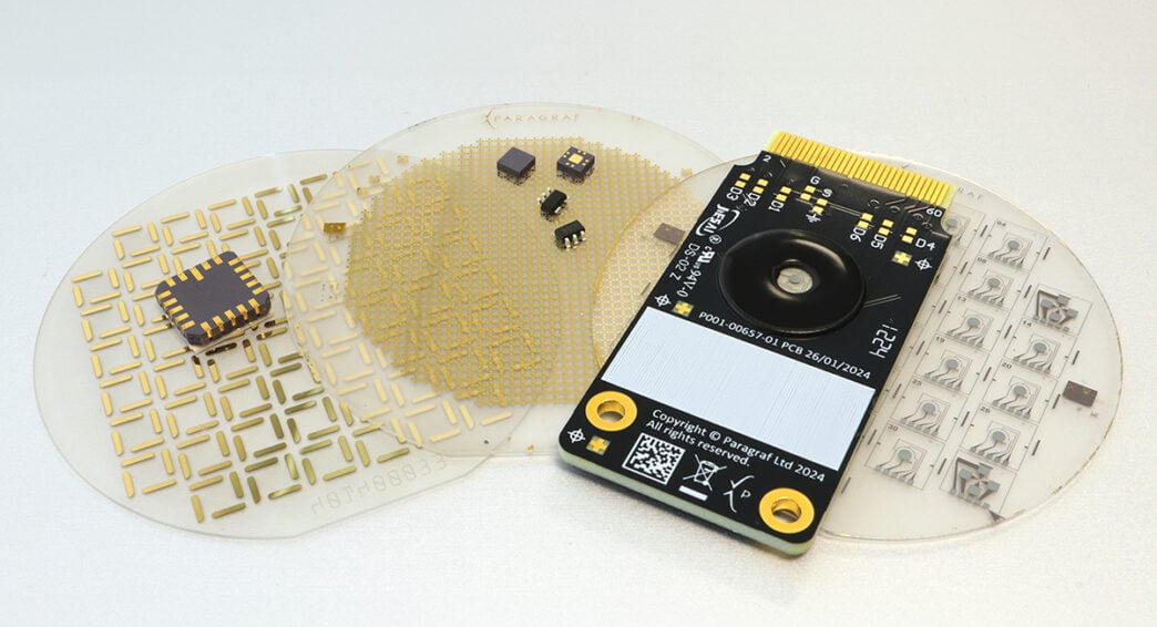
Paragraf has spent the better part of a decade developing a method to grow graphene directly onto standard semiconductor wafers – the same silicon, silicon nitride, and sapphire substrates used in conventional chip manufacturing. Using proprietary techniques to get the graphene on the substrate, everything else can be done with the same equipment you would find in any modern semiconductor fab.
“What we do is use a MOCVD [metalorganic chemical vapour deposition] deposition tool to deposit the graphene,” explains Dr. Hugh Glass, Paragraf’s Product Manager. “The chemicals we use, the recipes we use for that – that’s the proprietary bit. But once we’ve got the graphene on a substrate, we can then use standard tools to do photolithography, etching, and dicing up the wafer.”
This is big when it comes to commercial viability, owing to the amount of money that has already been pumped into the semiconductor industry, not to mention the uphill battle of trying to convince the industry to adopt an entirely new way of manufacturing. This is a classic case of don’t change your tools, change your materials, as Dr Glass explains: “Changing an industry like silicon, which has had billions of pounds put into it already, is quite difficult. So we want to make sure that anything we do is compatible with the manufacturing systems that already exist.”
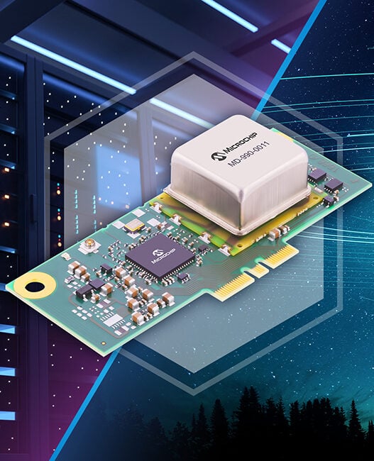
The memory problem
Paragraf has begun exploring graphene’s potential in data centre memory, which is more important now than ever, via a project funded by Innovate UK, the government’s innovation agency, and in partnership with Professor Judith Driscoll’s group at the University of Cambridge.
The project looks at ferroelectric memory. These devices combine graphene with ferroelectric materials, which can retain their state without continuous power. The combination, in principle, could produce memory that is faster, cooler, and less power-hungry than what data centres currently rely on.
Dr Glass explains that the ferroelectric layer matters because it provides the non-volatile switching behaviour that enables memory to retain information without constant power. Pairing that with graphene’s electrical transport properties creates the potential for memory devices that are robust, energy-efficient and fast.
The team is investigating two broad directions. One focuses on reducing energy consumption per memory operation, directly relevant to the power budgets of AI infrastructure. The other looks at how the material combination could support new architectures that blur the boundary between memory and computation, which is an area of growing interest as AI demands more distributed and efficient ways of processing information.
Resetting the roadmap
Dr Glass explains that silicon’s roadmap – the trajectory of performance improvements that the industry has relied on for fifty years – is effectively exhausted at the material level. Every recent advance has come from engineering around the material’s limitations, not from the material itself getting better.
Switching to graphene, Dr Glass says, resets this: “All of the changes that have been done recently for improvements are to do with architecture changes … in order to eke out the last bit of extra benefits from silicon. Whereas switching to graphene resets that, and we go back to having improvements due to the material before you even get to the architecture.”
Not only this, but reduced energy consumption means less heat is generated, so less cooling infrastructure is required. In hyperscale data centres, where power and cooling costs are a huge operational expense, even incremental device-level improvements could lead to big savings when considered at scale.
Dr Glass explains: “Power and heat are now first-order design constraints in computing infrastructure. Any new memory technology must demonstrate clear advantages in energy efficiency and thermal management to justify adoption.”
Innovating a concept
The Innovate UK project is a route to prove that the concept can be realised at a manufacturable scale.
“Historically, much graphene research has focused on proof-of-principle devices made using transfer processes or laboratory-scale fabrication methods,” Dr Glass explains. “Our approach is fundamentally different because we start from manufacturability.”
For Dr Glass, success at this stage means hitting three things simultaneously: being able to build the device structure reliably, demonstrating a clear performance advantage over existing memory technologies in terms of power consumption, and showing that the manufacturing method is repeatable and scalable rather than a one-off result.