
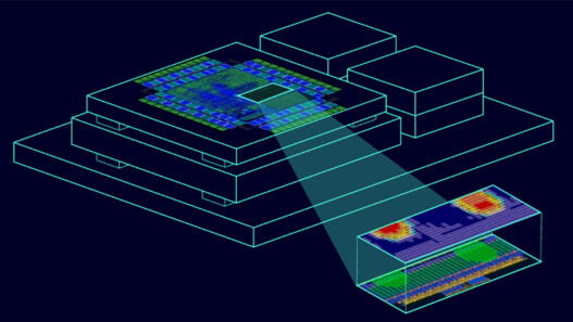


An isolated flyback controller is at the heart of many modern power supplies, enabling efficient energy conversion while safely separating high voltage inputs from sensitive outputs. This isolation is crucial for protecting users, reducing electrical noise, and meeting strict safety standards. Beyond safety, flyback controllers offer a compact, cost effective way to handle wide input voltage ranges and multiple outputs. That combination of simplicity, flexibility, and reliability is why isolated flyback designs are so widely used from consumer adapters to industrial and medical systems.
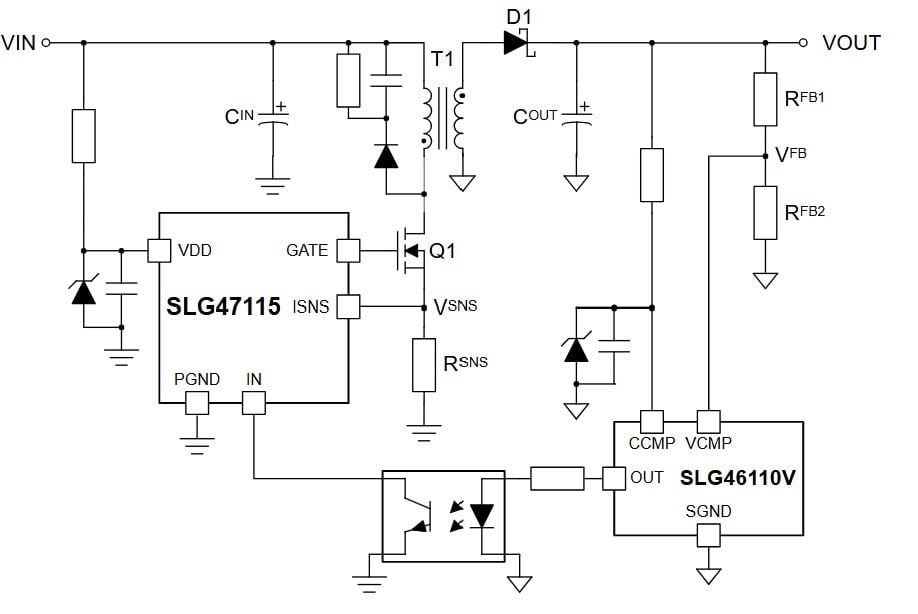
This article is based on AN-CM-420 SLG47115 and SLG46110V Isolated Flyback Controller and explains how to design and build an isolated DC-DC flyback controller using the SLG47115 as a low-side N-MOSFET controller and using the SLG46110 for isolated feedback via an optocoupler. It comes complete with Go Configure Software Hub design files as well as an Excel-based calculator tool for creating other flyback regulators with varying sets of input voltages, output voltages, output currents, and switching frequency ranges.
Flyback converter design and operation
Theory of operation
Each switching cycle begins when the voltage at VFB triggers the voltage comparator in the SLG46110. The optocoupler and the SLG47115 turn on Q1 and current ramps up in T1’s primary. Output diode D1 is reverse-biased while current flows in the primary. The current comparator inside the SLG47115 senses the primary current through RSNS at VSNS and turns Q1 off when the current reaches a peak value set by the user. The voltage in the secondary reverses direction, forward biases D1, and current flows to the output. The instantaneous voltage across the output capacitor COUT initially rises but then falls as the load discharges COUT. This causes VOUT and VFB to fall until SLG46110’s VCMP trips once again, starting the next switching cycle. In this hysteretic control method with fixed peak primary current, the switching frequency varies inversely with output power.
Go configure software hub projects
Steady state
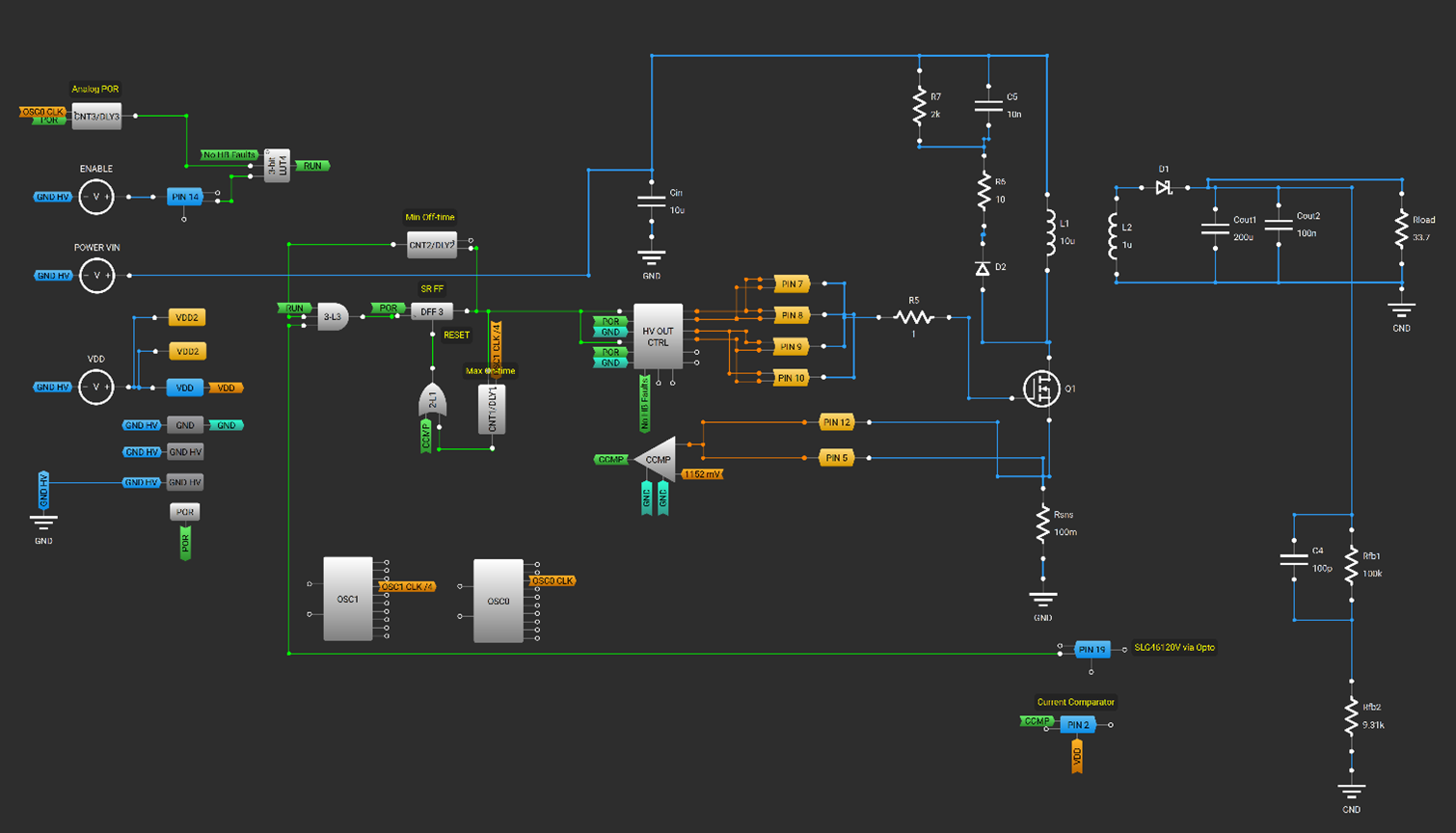
DFF3 is set as an SR flip flop with CLK as the SET input. In steady state DFF3’s output (Q) is set by PIN 19, coming the opto. The logic HIGH from DFF3 turns on the SLG47115’s internal half-bridges. This turns on Q1 and current rises in the primary of T1.
Once DFF3 is set the Max On-time counter (CNT1/DLY1) begins. Normally the fast current comparator CCMP resets DFF3, but if it fails to do so, CNT1/DLY1 is OR’d to DFF3’s RESET pin. This limits the on-time to 20µs. The user sets CCMP’s threshold from 4 up to 504mV. This along with the sense resistor RSNS sets the peak currents.
When CCMP or CNT1/DLY1 resets DFF3 the SLG47115’s half-bridges turn off Q1. CCMP has a typical response time of 350ns and there is an additional propagation delay in the digital gates of around 300ns. Total tCCMP is 650ns.
When CCMP has tripped current flow in the primary stops. The logic LOW at DFF3’s Q output also starts the Min Off-time block (CNT2/DLY2). CNT2/DLY2 prevents off-times of less than 2.52µs and provides some noise immunity for the SLG46110’s comparators. CNT2/DLY2 also limits the max switching frequency and ensures that a minimum energy transfer on each cycle.
In the SLG46110’s VCMP and CCMP outputs are OR’d together so that either one can turn Q1 back on.
Using a fast optocoupler
The RV1S9160A was selected for its 3.3 to 5V operation and propagation delay of 60ns max, HIGH to LOW or LOW to HIGH. The photodiode uses just 3mA of drive current, and no pull-up resistor is needed at its output. During startup when no drive current is available at the photodiode side, the RV1S9160A’s output stage defaults to a logic HIGH.
Designing with peak current hysteretic control
Electrical specifications
The example circuit:
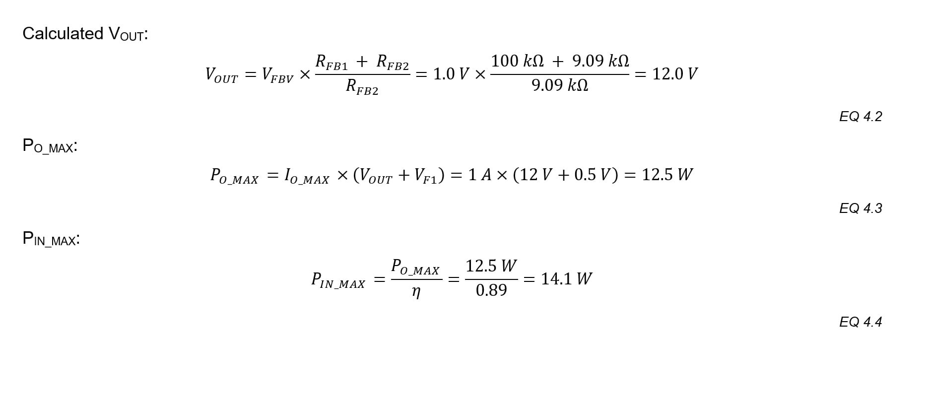
- VIN_MIN = 10V, VIN_NOM = 12V, VIN_MAX = 14V
- VO_TGT = 12V ±2 %
- IO_MAX = 1.0A
- Estimated efficiency: η = 89% (at max load)
- Target frequency, VIN_NOM and IO_MAX: fSW_TGT = 150kHz
- Max VDS of Q1: VBR_DS = 80V
- Max reverse voltage of D1: VRRM_MAX = 60V
The following parameters of the SLG47115, SLG46110 and output diode have been assumed:
- SLG47115 CCMP response time (typical): tCCMP = 650ns
- Output diode: VF1 = 0.5V
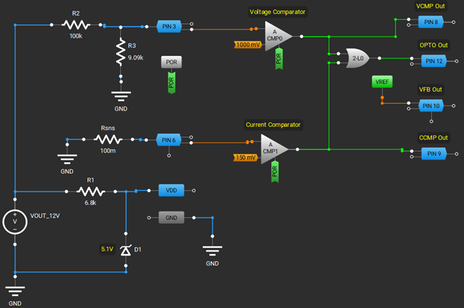
The inverting inputs of the SLG46110’s Voltage Comparator (CMP0) and Current Comparator (CMP1):
- CMP0 reference: VFBV = 1.0V
- CMP1 reference: VFBC = 150mV
The output resistors are selected first. 100 kΩ 1 % is a compromise between power dissipation and noise immunity for the upper resistor:
- RFB1 = 100 kΩ 1 %
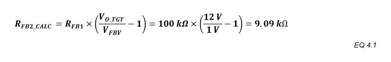
Using GreenPAK, a reference voltage can be selected to line up with standard tolerance values. 9.09 is an E96 1% value, hence the SLG46110-DIP comes with 1.0 V for VFBV:
- Lower resistor: RFB2 = 9.09 kΩ 1 %
Transformer design and peak primary current selection
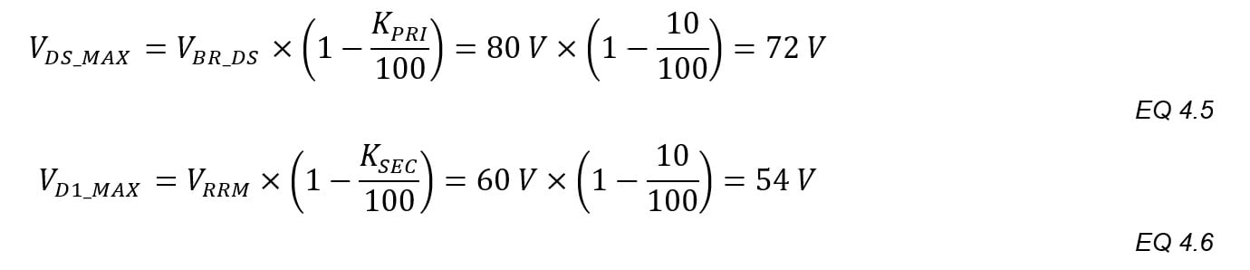
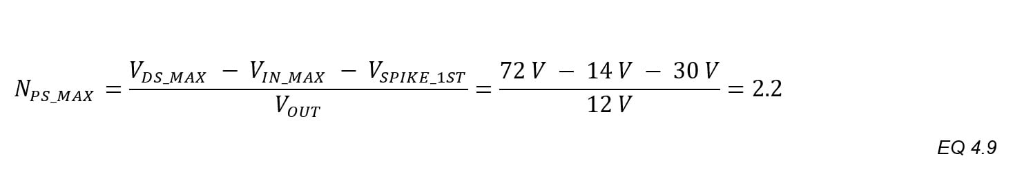
First select de-rating factors for Q1 and D1. For voltages < 100 V, typical de-ratings are 10%:
- Q1: KPRI = 10%
- D1: KSEC = 10%
The max voltages for Q1 and D1:
An estimate is needed for the leakage inductance spike. A clamping circuit is needed to prevent this transient from exceeding Q1’s VBR_DS. One design method is based on setting the target clamp to the midpoint between VIN_MAX and VDS_MAX:
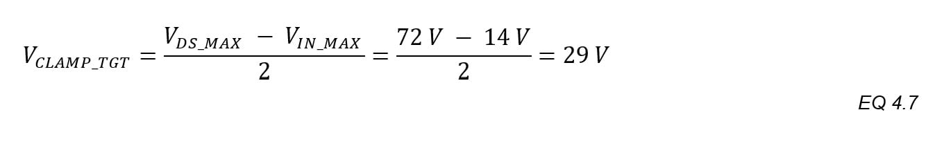
- VCLAMP_TGT = 30V
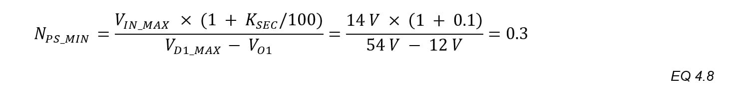
The min primary-to-secondary turns ratio prevents D1 from over-voltage:
The max turns ratio keeps Q1 from over-voltage:
Often the best target turns ratio is midway between the min and max, ~1.2:1. Here, an off-the-shelf flyback transformer with a ratio 1.33:1 was found.
- NPS_TGT = 1.33:1.
The voltage reflected to the primary while the secondary conducts:
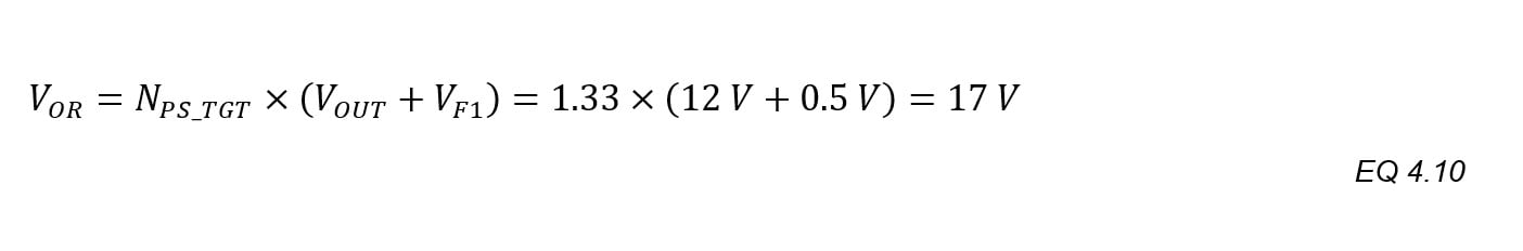
VOR must be less than VCLAMP_TGT or the circuit will clamp the reflected voltage from the secondary during core de-magnetization, likely overheating and damaging the clamp components. As 17 V is less than 30 V, this is a non-issue.
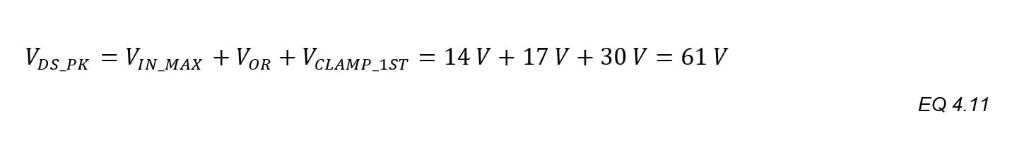
Peak predicted voltage across Q1:
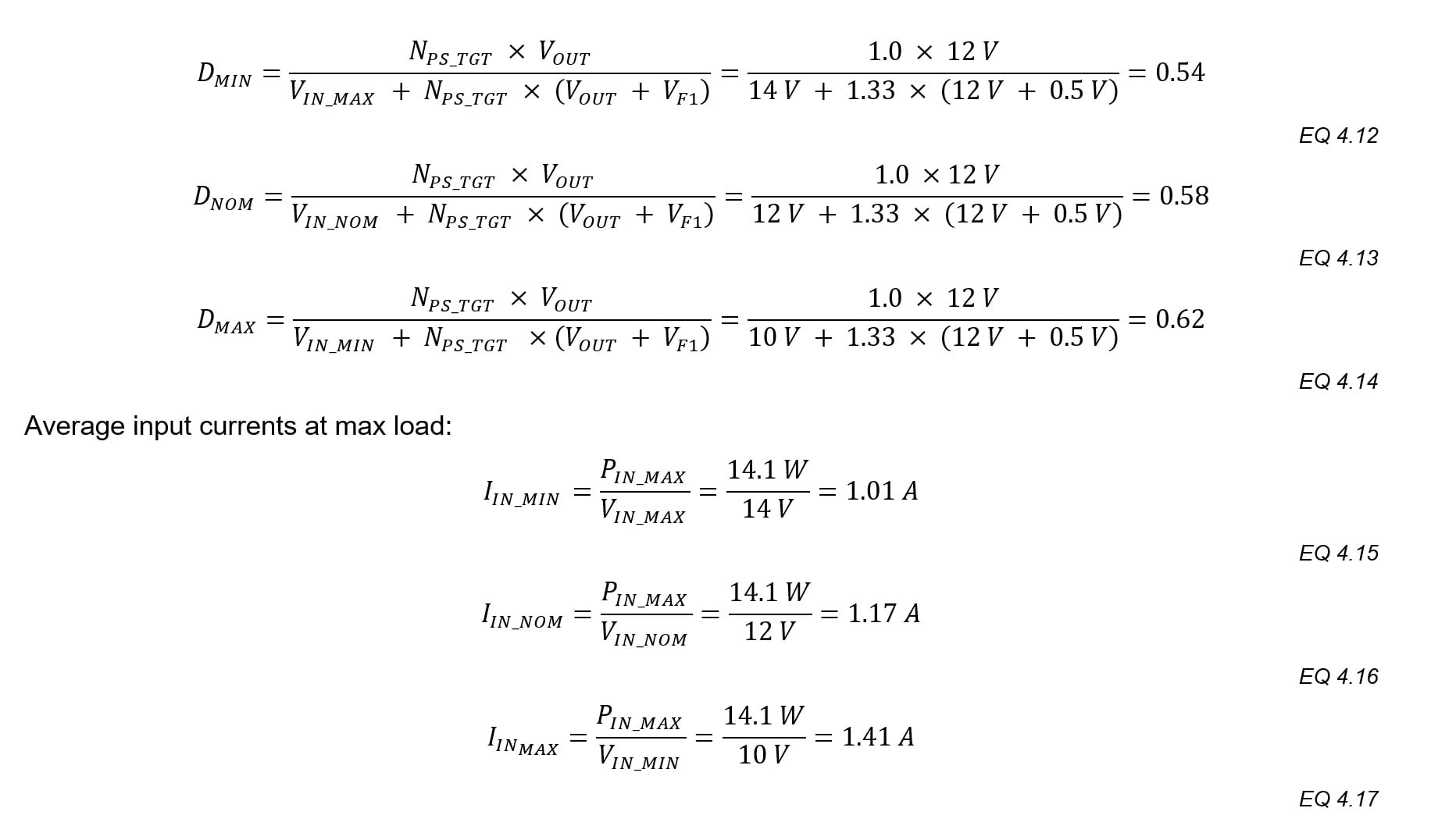
Primary magnetising inductance selection starts with the duty cycle. In continuous conduction mode (CCM), the duty cycle varies little with the output current or the frequency. Estimated duty cycle over VIN:
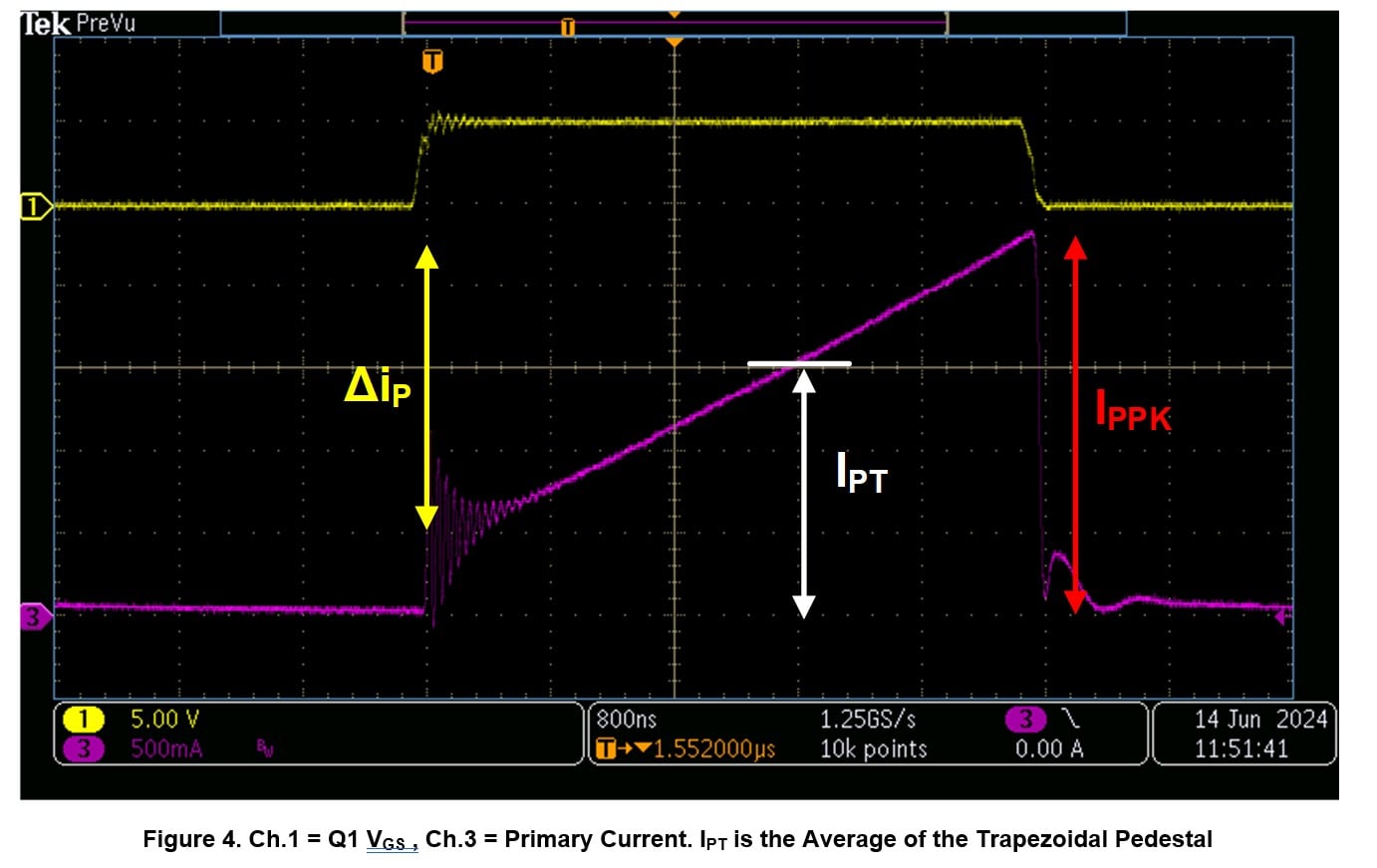
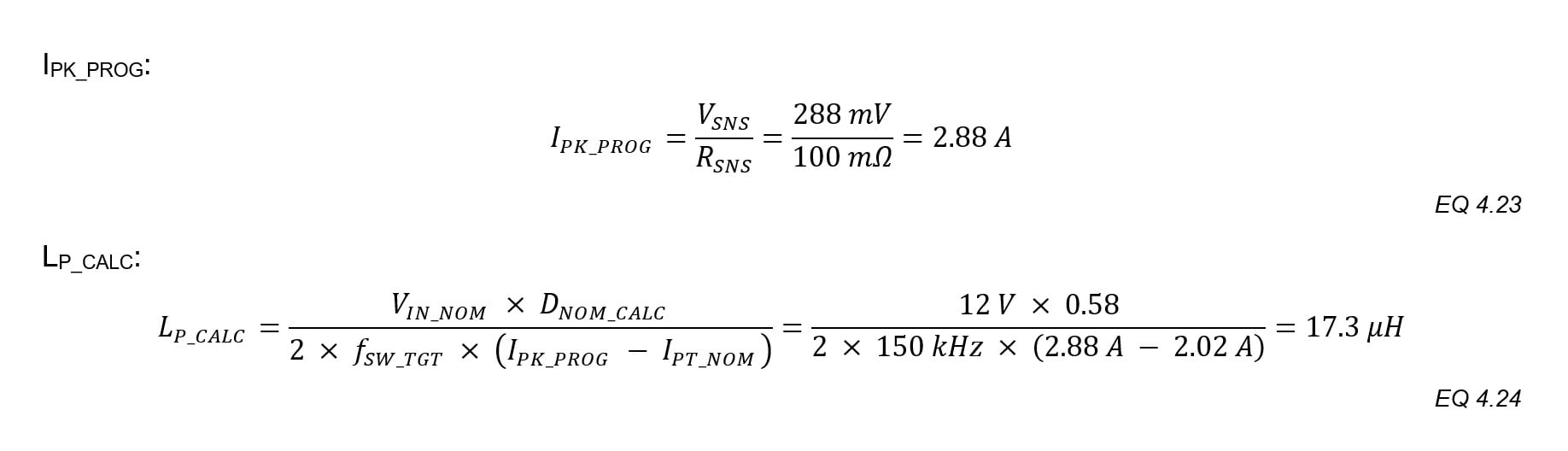
CCM flyback converters have trapezoid-wave primary and secondary currents. Inductance is selected to meet a target ratio of the average of the trapezoid’s pedestal to the peak and valley of that pedestal, see Figure 4.
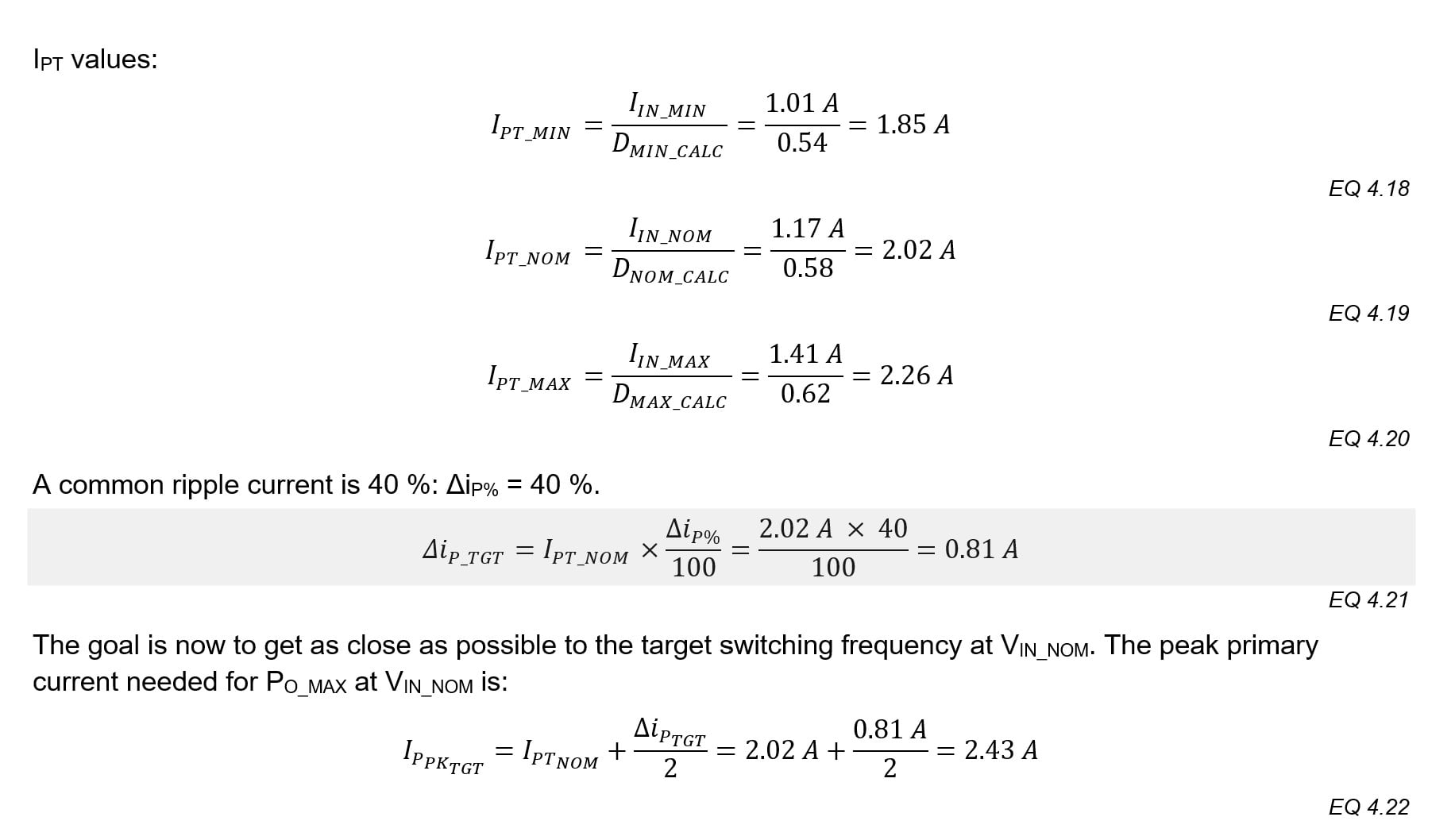
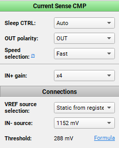
The user programs the actual peak current by selecting the current sense voltage and the sense resistor. Starting with a current slightly above IP_PK_TGT is recommended. A sense voltage of 100 to 500mV provides a balance between good accuracy and low power dissipation at this power level. 100mΩ is available with 1% tolerance in many sizes and powers.
- RSNS = 100 mΩ 1 %, size and power TBD
Figure 5 shows the final VSNS selection of 288mV.
A custom transformer could be exactly 17.3µH with a tolerance of ±10%. In this case the off-the-shelf Würth Elektronik 7491195212 has an LP of 21 µH. This higher inductance will affect the ripple current and therefore the frequency, but an off-the-shelf transformer saves development time.
- LP = 21 µH, ±10%
The 650ns (typical) total response time for the CCMP is a source of error in the peak primary currents during turn-off. These 650 ns are added to the calculated on time and yield higher peak primary current. The increase varies with VIN:
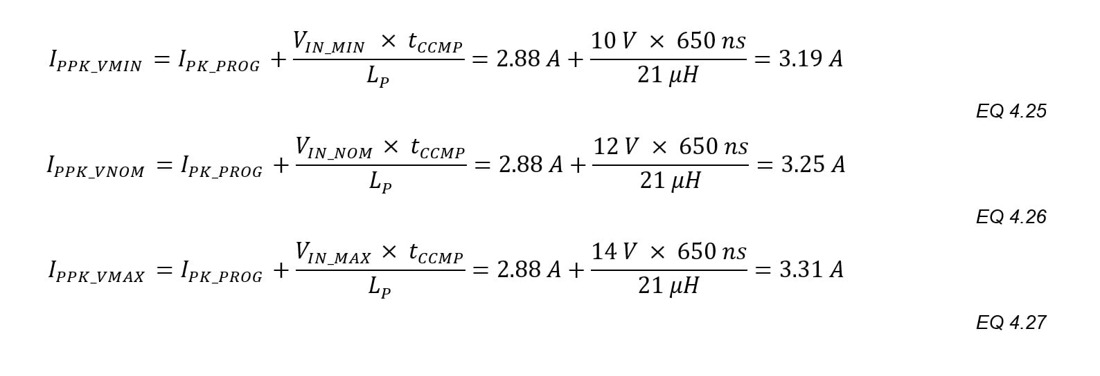
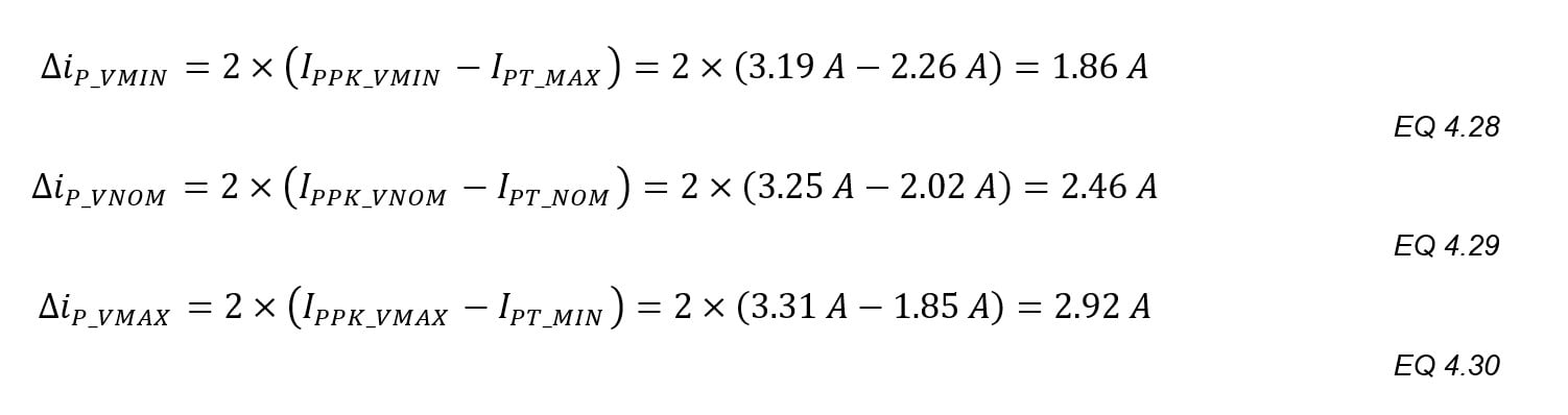
The peak-to-peak primary ripple currents:
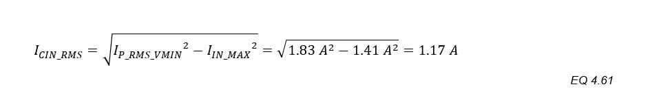
The highest RMS current is at VIN_MIN. This is used to calculate the conduction losses in Q1:
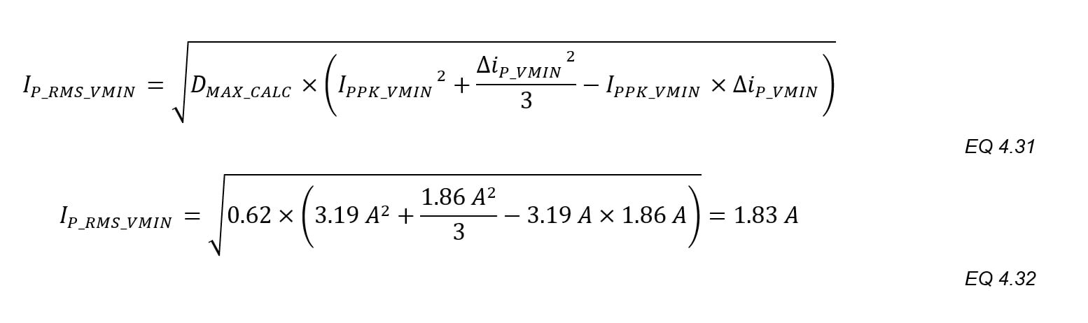
The RSNS power dissipation is 1.83A2 x 100mΩ = 0.33W. A single 0.5W, 1206-sized thick-film resistor will be used.
Next is core selection, then primary and secondary windings. A magnetic flux density of 0.3T is a common for general-purpose power supplies.
- BMAX = 0.3T
The effective core cross-sectional area is needed. Core volume is proportional to output power, and after a few designs a range of core shape and size combinations can be drawn from experience.
The Würth 7491195212 uses an EP13 core with an effective cross-sectional area, AE, 20mm2. The EP13 shape has two materials that would be good candidates: 3C96 from Yageo-Ferroxcube and N87 from TDK-Epcos, based on power loss versus flux density and power loss versus frequency.
- Core: EP13 – 3C96 or N87
- AE = 20mm2
Next comes the minimum number of turns. Peak primary current has been carefully set, so the design will be more accurate using the primary turns:
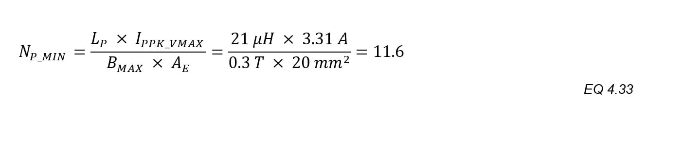
When the turns ratio NPS_TGT is greater than “1”, divide the result of EQ.4.33 by NPS_TGT to find the minimum secondary turns, and then select the next highest whole number. This generates results with whole numbers of turns.
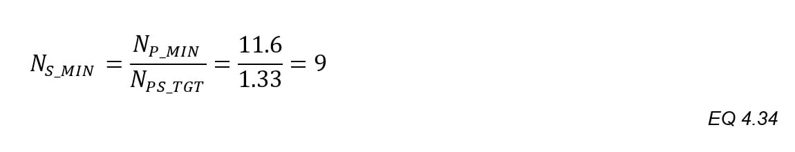
The next highest whole number is nine:
- NS = 9.
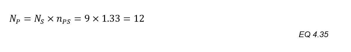
- NP = 12.
With hysteretic peak current mode the worst-case peak current is well-defined. Checking the peak flux density in the core:
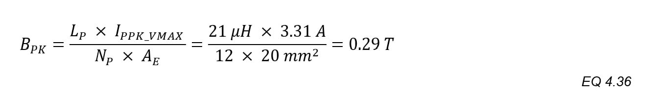
This is below the limit of 0.3T.
The secondary inductance and currents are now evaluated. Secondary inductance:
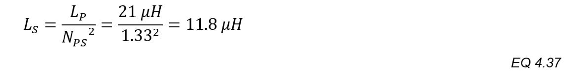
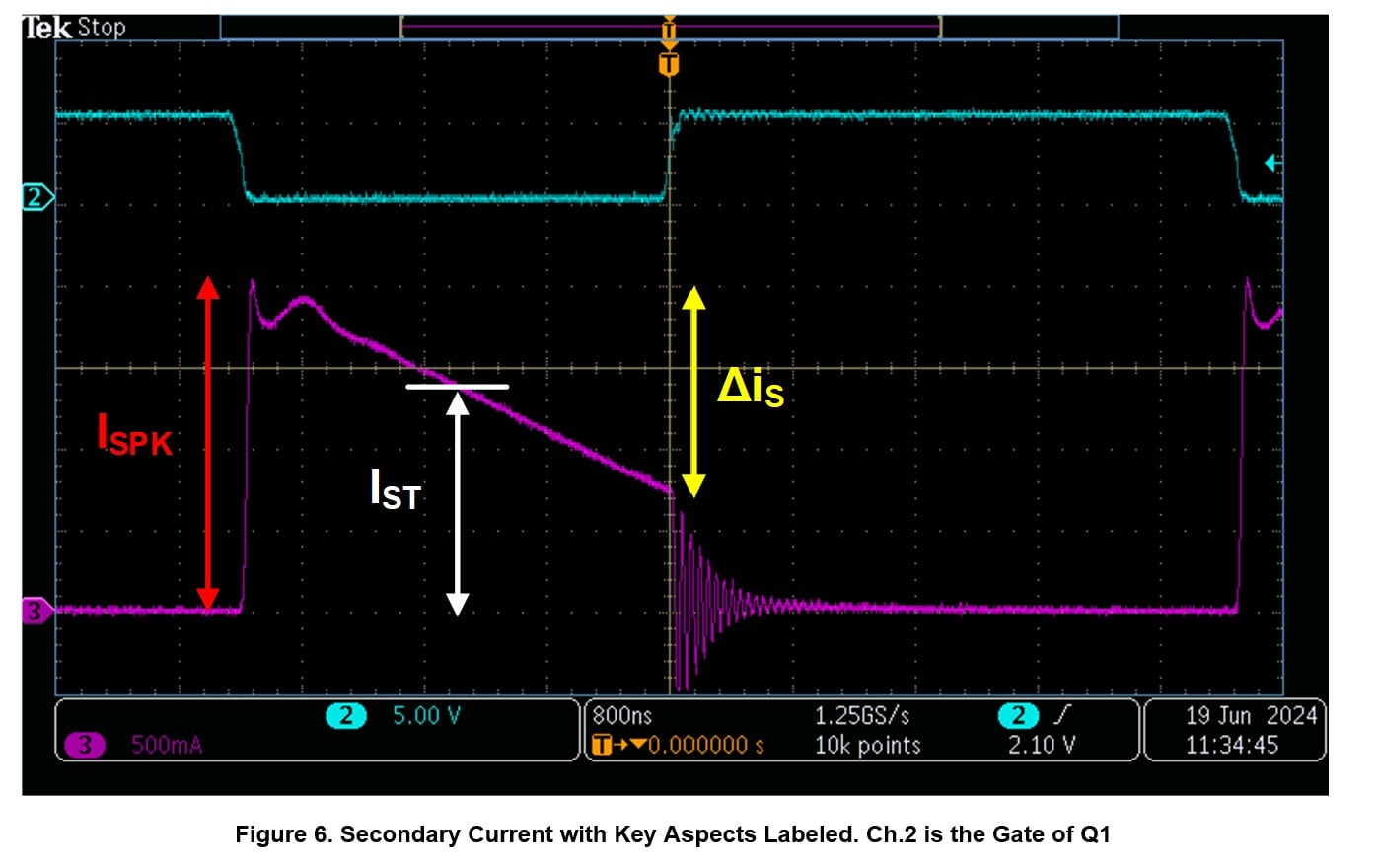
The worst-case secondary RMS current is used to predict the losses in D1 and in calculation of the AC ripple current in the output capacitor(s). The highest secondary RMS current occurs at the maximum input voltage:
T1 specifications:
- Core shape and size: EP13
- Core material: 3C96, N87, or equivalent
- LP = 21 µH, ±10%
- NPS = 1.33:1
- NP = 12
- NS = 9
- Peak primary current: 3.31A
- Max RMS primary current: 1.83A
- Peak secondary current: 4.42A
- Max RMS secondary current: 1.72A
Timing, duty cycles, and switching frequency
With T1’s inductances and currents calculated, the on-times (when Q1 conducts) and off-times (when D1 conducts) are re-evaluated more accurate duty cycle and switching frequency predictions.
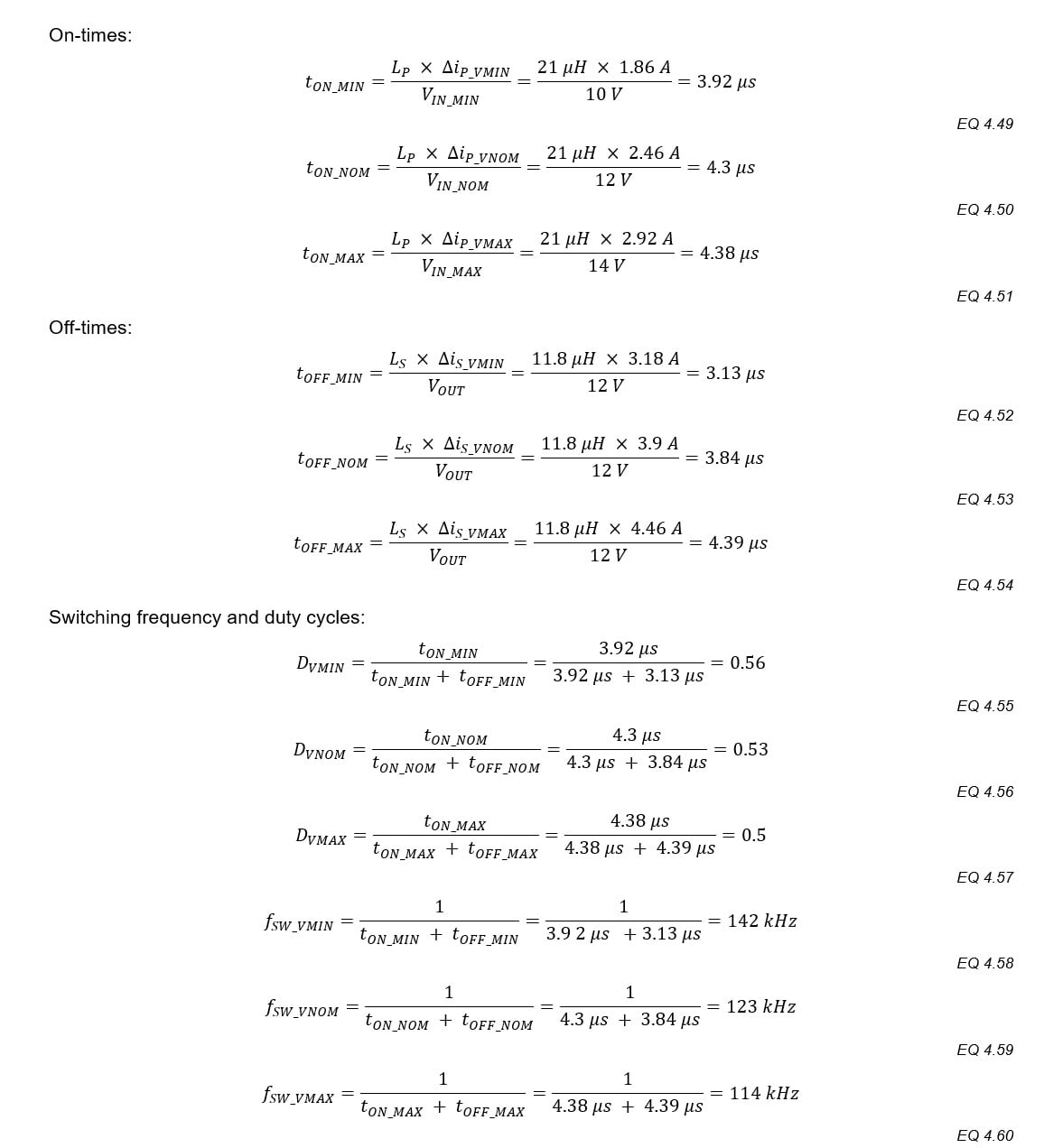
The initial target frequency at VIN_NOM was 150kHz. The combination of higher LP and the delay from the SLG47115’s current comparator induces error. Now, the designer can change the transformer or continue with the lower frequency. Variable frequency is needed in hysteretic control, so the lower frequency is found acceptable. Note: EQ 4.58, EQ 4.59 and EQ 4.60 predict the actual switching frequency at max load with good accuracy, as shown in Figure 18.
Input capacitors
The input capacitors endure high AC current from the trapezoid-wave currents they must supply. Figure 4 shows this waveshape, and the input capacitor’s current is similar but centred around zero. The following calculations provide a min total input capacitance and max total ESR, but in most cases the key specification is the AC ripple current rating of the combined input capacitor bank. When capacitor types with an electrolyte are used, their lifetime is reduced by the heat from the AC ripple current and their ESR. Maximum AC ripple current occurs at VIN_MIN:
The aluminium electrolytic (Al-E) capacitor should have a total RMS current rating greater than 1.2A at ≥ 100kHz. Using two capacitors in parallel splits the ripple current and is often cheaper and/or smaller than one large capacitor.
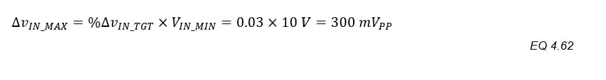
The max input voltage ripple is often not defined as clearly as ΔvO. Using 3% peak-peak of VIN_MIN is a good start. This prevents ΔvIN from affecting all the previous calculations that assume VIN is constant over the switching cycle.
- %ΔvIN_TGT = 3 % of VIN_MIN, peak-peak
CIN_MIN and ESRMAX are calculated based on ΔvIN_MAX. The factors of “2” assume that half of ΔvIN comes from the discharging of the input capacitors and half from IP_PK flowing through the ESR.
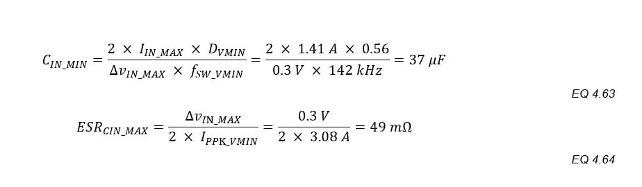
The next highest E6 value is 47 µF, but there are few 25 or 35V Al-E capacitors that meet the ESR requirement and none that meet the ripple current requirement. ESR drops and ripple current rating rises as the size of Al-E’s increases, and with larger size comes higher capacitance. So, the actual CIN will be greater than CIN_MIN so that the ESR and ripple current ratings are met.
In addition to using a larger Al-E rated at 330µF, 35V, 60mΩ, 1.19 ARMS @ 100kHz, the input to this circuit will also have one nominal 10 µF, 25 V, 1206, X7R and one nominal 100nF, 50V, 0603, X7R MLCCs in parallel. All three of these capacitors combine to keep the input impedance low over a broad range of frequencies. The 10µF MLCC will absorb some of the RMS ripple current and extend the lifetime of the Al-E.
A first-order estimation of ΔvIN can be calculated by first determining the impedance of the Al-E and then multiplying it by IPPK_VMIN. Real lab results will diverge due to factors such as ESL and the loss of capacitance as the frequency increases – lab testing is essential.
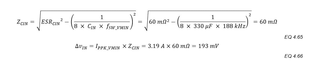
Figure 44 in section 5 Typical Performance shows that the actual ΔvIN under the worst-case conditions of VIN_MIN and IO_MAX is right around 200 mVP-P.
Output capacitors
The output capacitors in a flyback converter also contend with heavy RMS ripple currents from the trapezoidal secondary current. The RMS value of the output capacitor ripple current is:
The same aluminium capacitor used for the input will be used at the output. Due to the heavier ripple current and lower max ESR, two 330 µF Al-Es are used in parallel.
- Total output capacitance: COUT = 660µF
- Total ESR: ESRCO = 30mΩ
One 10 µF, 25 V, X7R, 1206 and one 100 nF, 50 V, X7R, 0603 MLCC are placed in parallel. With their small size and low ESL, their main job will be to filter high frequency parasitic oscillations and transients.
The output voltage ripple estimation:
The predicted ripple looks much lower than the limit on paper, but lab testing without the 10 µF MLCC C16 showed higher ripple due to parasitic capacitances and inductances in the components and the PCB, shown in Figure 7.
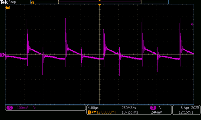
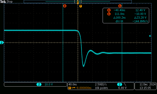
In contrast, Figure 28, Figure 30, and Figure 32 show the lab tested results for output voltage ripple at a 1A load with C16 for VIN = 10, 12, and 14V respectively. Switching frequency ripple is around 80 to 90 mVP-P and the high frequency parasitic oscillations from Figure 7 that increased the total ripple to nearly 500 mVP_P are absent.
Primary N-MOSFET, Q1
Selecting Q1 starts with the gate drive voltage. Using the same 5V for the VDD pins keeps the system simple and power dissipation low. Never use any MOSFET that isn’t rated for 5V gate drive. Parts rated for higher VGS may not fully enhance.
The 80 VDS RJK0852DPB was selected for its 4.5VGS rating and balanced switching and conduction loss. The following equations are generally accurate when selecting relative FET loss, but not for absolute loss. Lab testing is mandatory for FET loss.
Datasheet values:
- RDSON_MAX 4.5 VGS, TA +25ºC
- Typical output capacitance, COSS
- Typical reverse transfer capacitance, CRSS
- Typical gate-to-drain charge, QGD
- Typical total gate charge, QG
The SLG47115’s peak gate drive sink and source currents are needed. If one half-bridge is used this is 3A for both sink and source, 6A for both half-bridges. This design uses both.
- ISOURCE = ISINK = 6A
The drain-source rise and fall times:
Primary output diode
Schottky diodes are preferred due to their low VF. From EQ 4.6 that the maximum reverse voltage is 54V, making 60V a good choice. Power dissipation:
Many 60V Schottkys are available. The most important factors are the package and thermal resistance. The TO-277A has large thermal tab relative to its footprint. Select a diode with a continuous forward current rating that is at least equal to the peak secondary current, ISPK_VMAX, 4.4 A. Figure 8 shows the secondary switch node at 1A load and VIN = 10V.