


Antenna performance is never just about the antenna itself. The PCB beneath it plays an equally critical role in determining range, efficiency, and overall wireless reliability.
Even the most sophisticated antenna can fail if the PCB layout isn’t designed to support it. In any modern wireless device, the printed circuit board plays an active role in the antenna’s performance, shaping radiation patterns, affecting impedance matching, influencing efficiency, and even determining whether the product meets regulatory requirements. Too often, the PCB is treated as an afterthought, addressed only after the mechanical and digital design decisions have been made. But by understanding that the board is part of the antenna system itself, not just a carrier for components, engineers can dramatically improve wireless performance, shorten development cycles and avoid costly redesigns.
The PCB and antenna: a shared radiating system
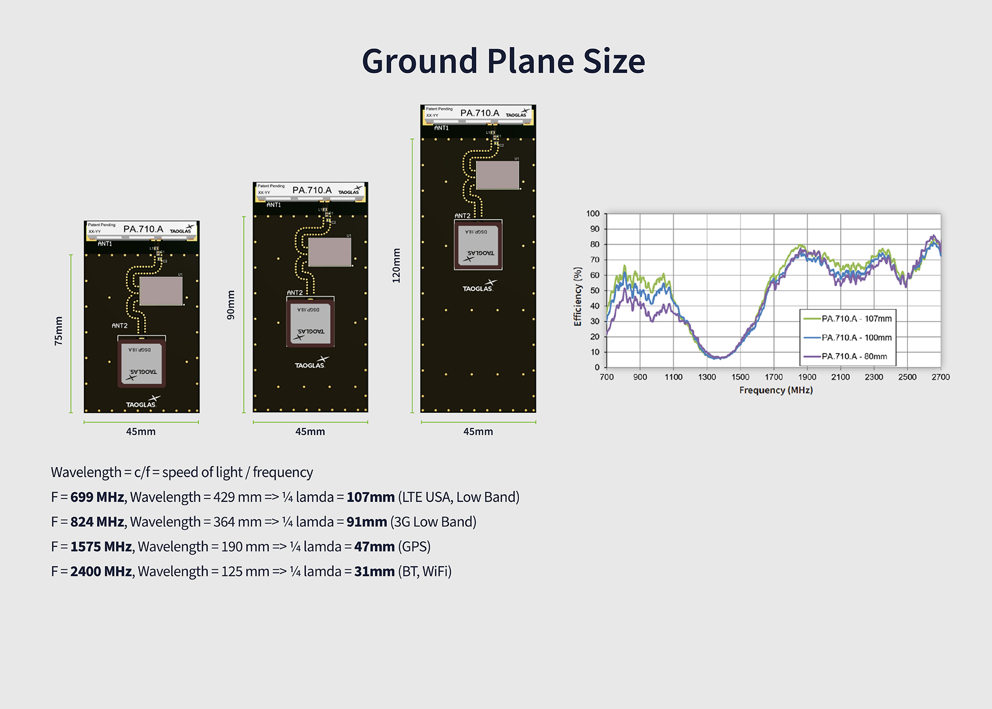
Antenna efficiency is not determined by the antenna alone. The PCB is effectively part of the radiating structure, often serving as a counterpoise or completing the electrical length of the antenna. For common embedded types such as monopoles or planar inverted F antennas (PIFAs), the size, shape, and continuity of the ground plane directly affect radiation patterns, impedance and efficiency. A ground plane that is too small or fragmented will reduce bandwidth and gain, while a poorly shaped one can distort radiation lobes or create mismatch losses.
A useful rule of thumb is to size the ground plane (usually the longest edge of the board) to about a quarter wavelength at the lowest operating frequency, which helps the antenna and ground together achieve the required half-wavelength resonance. For example, a device designed for 700MHz LTE ideally needs around 108mm of ground length. Higher-frequency systems, such as 2.4GHz Bluetooth or Wi-Fi, have shorter wavelength requirements, but multiband devices must often accommodate the lowest band’s physical constraints. Where space is limited and a full quarter wavelength is not achievable, aiming for at least a 70 × 70mm ground plane can deliver acceptable performance, and further compromises can be mitigated through careful matching and layout discipline, but these often come with trade-offs in performance.
Antenna placement is another key system-level consideration. Patch antennas generally perform best when centred on the PCB ground plane, which promotes symmetry and predictable radiation patterns. Monopole-type designs often benefit from placement near the board edge, where the ground acts as the counterpoise or return path for the antenna. Mechanical elements, from battery housings and display frames to mounting holes and shield cans, can all influence the electromagnetic environment, so decisions about where the antenna will sit must be made early in the design cycle.
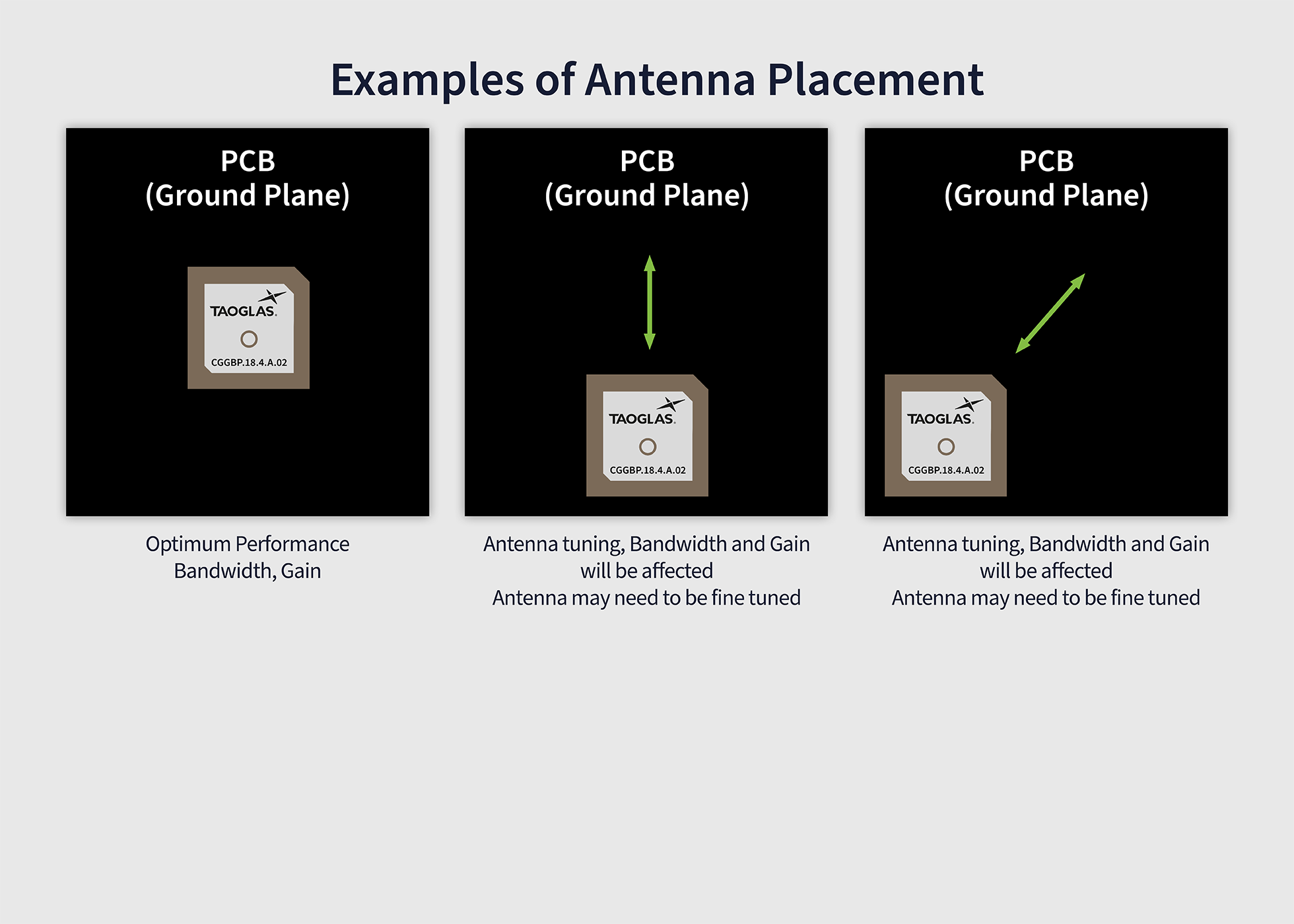
Clearance around the antenna is equally important. A well-defined keep-out area, free from copper, traces, components and vias, prevents detuning and performance degradation. Proximity to large conductive objects, particularly batteries or metal enclosures, can absorb energy or shift resonance frequencies. Taoglas typically recommends keeping such objects at least 20mm away, though the exact figure depends on frequency and antenna type. Even dielectric materials such as plastic enclosures or display glass can have subtle but significant effects, underlining the need for close collaboration between RF and mechanical design teams.
Transmission lines, matching, and tuning
Delivering power to the antenna efficiently requires meticulous attention to the RF feed structure.
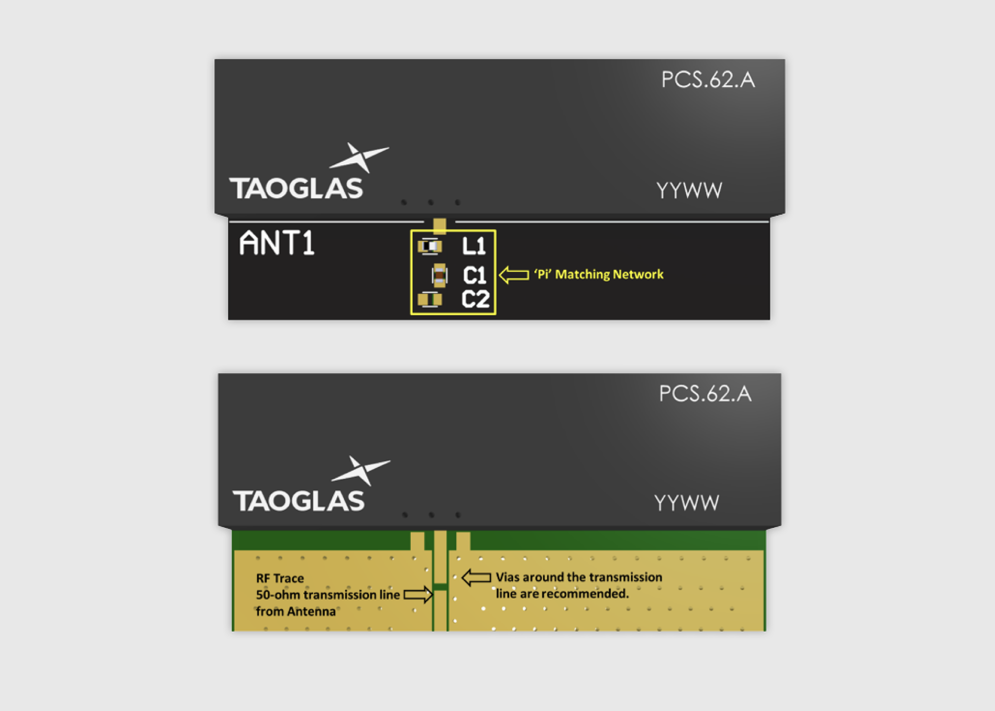
The transmission line, whether implemented as microstrip, coplanar waveguide or grounded CPW, must maintain a controlled 50Ω impedance, with trace width and spacing calculated according to the PCB’s stack-up and dielectric properties. Abrupt bends, unnecessary vias and impedance discontinuities should be avoided to preserve signal integrity. A solid ground reference, implemented with stitching vias and continuous copper, helps suppress parasitic effects and reduce unwanted coupling.
The matching network is another vital part of the system, not just for initial impedance matching but also for fine-tuning. A Pi or T configuration is common, but the key is flexibility: leave sufficient space for additional components or alternate values during development. In almost every real-world design, prototype tuning is required once parasitics, manufacturing tolerances and housing effects are accounted for. Using high-Q, RF-rated inductors and capacitors with minimal parasitic resistance or reactance improves predictability across temperature and frequency.
Even with a well-designed layout, simulation and measurement are essential. Full-wave electromagnetic simulations can reveal current distributions, field coupling and the influence of nearby structures before hardware is built. Circuit-level simulations of the matching network, including realistic component tolerances, help predict how performance might vary in production. Once prototypes are available, vector network analyser (VNA) measurements of S11, return loss and impedance provide early validation. Anechoic chamber tests can then assess gain, radiation patterns, total radiated power, and overall system efficiency. Comparing these results against simulation data allows engineers to fine-tune the design and matching network iteratively.
Avoiding pitfalls and achieving right-first-time designs
Many wireless performance issues trace back to recurring design mistakes. One of the most common is treating the antenna as a discrete component rather than a system-level design element. This leads to compromised placement, insufficient clearance or fragmented ground planes that limit efficiency. Another frequent oversight is failing to plan for tuning; even antennas designed to perform well over a range of ground sizes benefit from adjustments once real-world parasitics are introduced. Splits or gaps in the ground plane near the antenna region are another classic cause of degraded performance, as is routing noisy switching regulator traces or high-speed digital lines too close to the RF path.
Most of these problems are avoidable if RF considerations are integrated into the design process from the outset. Early collaboration between hardware, RF, mechanical, and compliance teams ensures that critical decisions (antenna choice, placement, clearance, ground structure, and routing) are made holistically rather than sequentially. It also means that simulation, prototyping and tuning can follow a more predictable and efficient path, improving the likelihood of achieving performance targets on the first design iteration.
Ultimately, antenna performance is a property of the entire system, not just the radiating element. The PCB, enclosure, components and even nearby materials all interact with the antenna’s electromagnetic fields. By approaching PCB design as part of the antenna, rather than a separate engineering task, designers can deliver products that perform more reliably, meet regulatory requirements with margin, and achieve the range and data rates expected in today’s wireless applications.

Engineering, Taoglas