


The AOLV66935 designed by Alpha and Omega Semiconductor is a 100V N-channel High Safe Operating Area (SOA) MOSFET in an 8 x 8 LFPAK package that handles higher peak currents and offers a cost-effective, high-performance, and more reliable hot-swap solution.
It features very low power-on resistance to meet the power demands of AI servers, which are intensifying primarily due to increased GPU/TPU performance.
The new MOSFET is available in AOS’s latest-generation LFPAK 8 x 8 package, which is 60% smaller than the TO-263 (D2PAK) package.
The AOLV66935 utilises AOS’s patented 100V AlphaSGT MOSFET technology, which combines the advantages of trench technology for low turn-on resistance with high SOA capability for linear mode operation.
Outstanding features
This device features advanced clip technology with a high current rating to provide high inrush current capabilities. In addition, the copper clip and packaging technology used offers low thermal resistance for improved thermal management.
Furthermore, the AOLV66935 provides low power loss and reduced heat generation due to its leading low RDS(ON) of 1.85 mOhms maximum rating at VGS=10V.
In line with the requirements of the latest AI server applications, the MOSFET is designed with advanced features and high-current capabilities necessary for improved thermal cycling under harsh conditions.
The AOLV66935 is specifically engineered for 48V systems, providing reliable protection and control in hot swap, load switch, and soft start applications.
Designers can meet the space constraints imposed by the design, thanks to the exceptionally low on-resistance of this device, which significantly reduces conduction losses, thus requiring fewer devices in parallel.
Technical characteristics
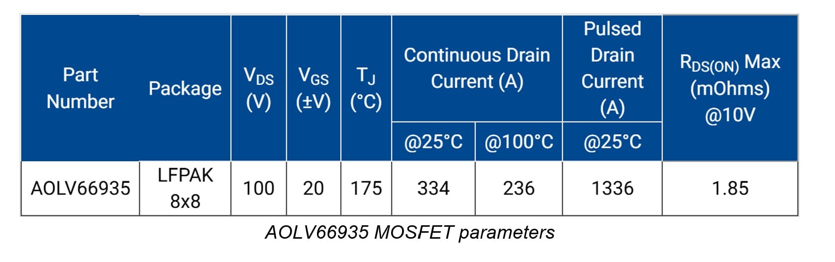
Key technical features of the AOLV66935 include a high continuous drain current of 334A at 25°C case temperature, a pulsed drain current of 1336A, and a maximum on-resistance (RDS(ON)) of 1.85 mOhms at VGS=10V, which significantly minimises conduction losses. It is housed in a compact LFPAK 8 x 8 package, which offers superior thermal resistance (RthJC of 0.35°C/W) and can operate reliably under extreme conditions with a junction temperature of up to 175°C.
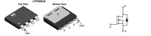
The image below displays a physical representation and schematic symbol of the MOSFET in a 4-pin LFPAK 8 x 8 surface-mount package, designed for high-SOA applications in AI servers.
The large metal tab on the bottom view is the Drain (D) terminal.
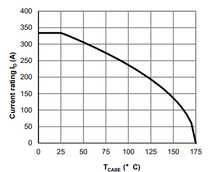
The next image displays a graph showing the current de-rating characteristics. It illustrates how the maximum allowable current decreases as the case temperature increases.
The current rating decreases linearly from 340A at 25°C to 0A at approximately 175 °C case temperature.
SOA performance
The figures below display the Safe Operating Area (SOA) for the AOLV66935 MOSFET, illustrating the maximum permissible current (ID) and voltage (VDS) combinations under various pulse conditions.
The operating area is bounded by RDS(ON) limits and specific pulse durations (10 µs to 100ms), showing one graph for TC = 25ºC and another for TC = 125ºC.
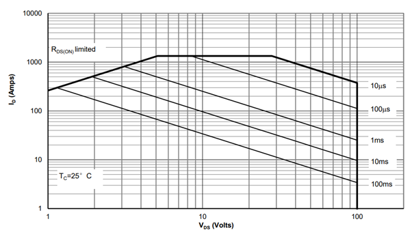
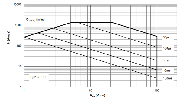
This curve is based on the junction-to-case thermal impedance, which is measured with the device mounted to a large heatsink, assuming a maximum junction temperature of TJ(MAX) = 175°C. The SOA curve provides a single pulse rating.
Switching characteristics
As seen in the following image, the switching characteristics of an AOLV66935 MOSFET power device are captured in an oscilloscope screen.
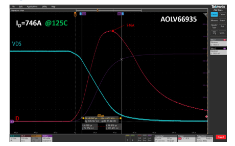
The test conditions involve a triangular waveform with a drain-source voltage (VDS) of 60V and a case temperature (TC) of 125ºC.
The total switching time is approximately 40 microseconds (µs).
The peak drain current (ID) reaches 746A at 125ºC.
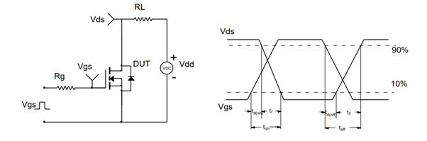
The diagram in the image shows a resistive switching test circuit that uses an AOLV66935 MOSFET transistor (Device Under Test, DUT) configured as a low-side switch.
The gate resistance (Rg) limits the charging and discharging current of the MOSFET’s internal gate capacitor.
The load resistance (RL), connected between the drain-source (Vds) and the source (Vdd), is where the voltage drop is measured to determine the on/off state.
Vgs and Vds are the gate-to-source and drain-to-source voltages, respectively.
The waveforms illustrate the MOSFET switching times when a voltage pulse is applied to the gate (Vgs).
Turn-on times:
• td(on) (turn-on delay time)
• tr (rise time) shows the drain transition from high to low, typically measured between 90% and 10% of the final voltage
• Ton (total turn-on time)
Turn-off times:
• td(off) (turn-off delay time)
• tf (fall time) shows the drain transition from low to high, measured between 10% and 90% of the voltage
• Toff (total turn-off time)
Suitable applications
Server
The AOLV66935 Hot Swap MOSFET is the ‘muscle’ within a server’s monitoring module. Its primary function is to act as a controlled on/off switch, allowing components (such as disks or power supplies) to be connected or disconnected from a powered backplane without causing failures in the rest of the system.
To use the AOLV66935 for inrush current control when a new component is inserted, the controller makes the MOSFET operate in linear mode (like a variable resistor) instead of allowing all the power to flow at once.
This way, the power increases gradually (soft-start), preventing sparking at the contacts and voltage drops that could reset other components in the rack.
MOSFETs designed for servers have an extremely low RDS(ON) (milliohms) to minimise power loss and heat generation during continuous operation.
To ensure reliability, these components must have a robust SOA (Safe Operating Area), allowing them to withstand high voltages and currents simultaneously during the insertion process without burning out.
Telecom infrastructure
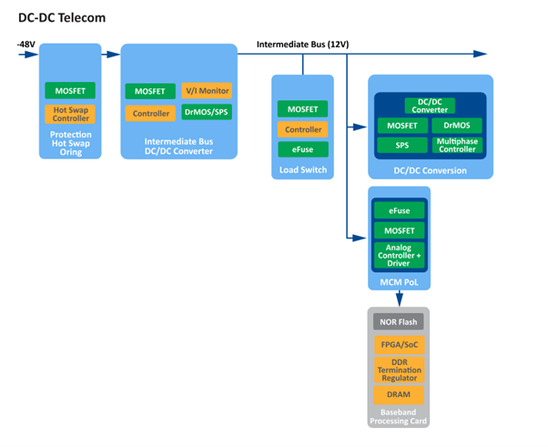
For its specific application in telecommunications infrastructure (generally -48V or 24V systems), the MOSFET must combine an extremely low on-resistance (RDS(ON)) with a robust SOA to withstand inrush currents without failing.
The AOLV66935 is a 100V MOSFET specifically optimised for 48V architectures. This component is designed to manage soft start and fault isolation in hot-swapped cards, allowing the telecommunications platform to remain operational while modules are being replaced.
For -48V systems in DC/DC telecom, the MOSFET must be able to dissipate considerable energy during the insertion event (where it acts as a variable resistor) and offer minimal resistance in steady state.
On the other hand, in a -48V system, the MOSFET faces high VDS voltages and inrush currents simultaneously during soft start. The AOLV66935 offers a robust SOA curve, vital for preventing silicon thermal failure. Its RDS(ON) of 1.85 mΩ drastically reduces voltage drop and heat generation, allowing for designs without bulky heatsinks.
The LFPAK 8 x 8 package is preferred in telecom applications due to its low inductance and high current capacity compared to the traditional D2PAK, while occupying 60% less PCB space. It offers superior thermal resistance and a low profile, making it ideal for server racks with restricted airflow.