


An almost entirely biodegradable circuit board has been developed and could help reduce the environmental harm of electronic waste.
Researchers from the University of Glasgow have developed a new method of printing zinc-based electronic circuits on environmentally-friendly surfaces, including paper and bioplastics.
The research aims to address the growing problem of electronic waste, or e-waste, caused by the materials used in the construction of modern electronic devices. Once the circuits are no longer needed, 99% of their materials can be disposed of safely through ordinary soil composting or by dissolving in widely available chemicals like vinegar.
Speaking about the project, co-author Dr Jon Harwell of the University of Glasgow’s James Watt School of Engineering, said that the research project was aimed at exploring biodegradability as a way to reduce e-waste footprints. The team focused on the PCB, as this makes up a major mass fraction and is known to be particularly hazardous.
Looking at the parts of it which could be made using biodegradable materials, Dr Harwell said: “The conductor and the substrate make up most of the mass of a PCB, so that’s where we decided to start – copper is toxic to cells so we can’t really use it for composting stuff so we explored other materials – zinc was the only one that seemed even remotely viable (all other biocompatible materials were either too unstable or too poorly conductive), but it’s still known to be very challenging to work with.
“The breakthrough came when I was playing around with electroplating zinc onto aluminium – I found if I did the exact opposite of all the conventional industry methods designed to maximise the adhesion of the zinc to the aluminium, then I could make a zinc pattern which could be easily peeled away from the aluminium while remaining intact. After that, it was easy to transfer it to basically whatever material we wanted.
“We still encourage e-waste to be processed through formal routes; zinc or copper, and also substrates should still be recycled where possible; this reduces mining activity and encourages sustainable behaviour.”
Zinc as a conductor
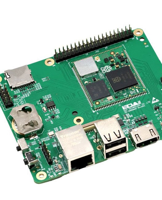
Conventional circuit boards are typically made from materials that are difficult or expensive to recycle at end of life, meaning they are often disposed of in landfill, where they can leach harmful substances into the surrounding environment.
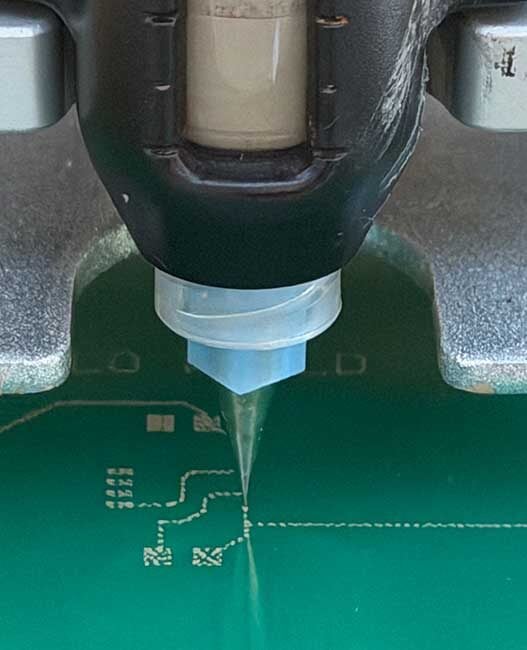
In contrast to traditional PCBs that rely on copper for electrical conduction, the researchers use zinc to form metal tracks just five microns wide. Conductive zinc is electroplated onto a temporary carrier before being transferred onto a biodegradable substrate, producing circuits that show comparable performance to conventional boards.
When talking about any trade-offs when using Zinc in terms of durability and manufacturability, Dr Harwell said: “For durability, we found that the Zinc is really stable in air (the first samples we made almost two years ago haven’t noticeably degraded yet), but like most electronic components, it degrades rapidly when wet.
“Zinc is normally much harder to manufacture (which is another reason why it’s not normally used), but our method makes it much easier to work with, and our method is also additive, which means that material is only used exactly where it is needed. As opposed to the way normal PCBs are made, which is by applying a blanket sheet of copper and removing the unwanted material, resulting in wasted copper.”
Zinc, however, is about a third of the conductivity and cost of copper, but, Dr Harwell says that it’s still more than conductive enough for most purposes, and, if it’s really necessary, then the reduced conductivity can be dealt with by increasing the thickness of the zinc, which, given its lower cost compared to copper, makes the price comparable to copper.
Expected lifespan
Speaking about the realistic lifespan of these circuits in deployed devices, particularly IoT or sensing applications, Dr Harwell said they expect the devices to have a shelf life of at least two years, but would need to do more real-world tests in order to prove that.
“We are specifically targeting short lifetime ‘disposable’ applications for things like smart labelling or applications such as electronic pregnancy tests. These have relatively short use cases, and it’s not very practical to reuse or recycle them. In these cases, we expect the stability of our devices to be more than sufficient, as they only need to match the shelf life of the sensing components within them (which is usually around a year in the case of pregnancy tests, for example).
“In practice, even copper isn’t stable without some organic coating to limit oxidation. We envisage the same for Zinc – an organic material that limits water/oxygen ingress will probably be needed for applications.”
The environmental impact
A life cycle assessment conducted by the team compared the potential environmental impact of their new PCBs against conventional boards. Their findings show that the biodegradable PCBs could enable a 79% reduction in global warming potential and a 90% reduction in resource depletion, suggesting that they could enable significant reductions in the environmental impact of electronic devices.
Dr Harwell said: “The work demonstrates a major step toward circular electronics, where devices are designed from the outset for reuse, recycling, or safe degradation. Discarded devices already generate tens of millions of tonnes of waste annually, so our research could have far-reaching impacts for consumer electronics, internet-of-things devices and disposable sensors in the future.
“One of the major benefits of our approach is the ‘additive’ nature of our method. Because our method only deposits the metal exactly where it is needed, we can get away with using a lot less metal than would be needed if we were etching patterns into a blank copper sheet, as is done in a conventional PCB etching process. This also avoids the need for harsh acids, which are normally used to etch the copper and thus produces less chemical waste.
“The other main contributor is the ability to use more eco-friendly substrate materials over the fibreglass composites, which are normally used. By using bio-derived materials such as paper, we can use more readily available materials (or even upcycle industrial by-products) while also reducing their e-waste footprint at their end of life.
“The key challenge remains in powering these devices. There isn’t much point in making a biodegradable circuit that is then powered by an expensive and non-degradable lithium battery. Hence, we are also working on degradable batteries that can be integrated into these devices made using materials such as zinc, carbon, and gelatine. This would give us a fully biodegradable, all-in-one solution for the applications we are targeting.”
Speaking on how controllable the degradation process is and what safeguards would need to be in place to ensure the devices do not begin breaking down prematurely in real-world environments, Dr Harwell said: “The key trigger for degradation in our devices is warm, wet conditions typically found in composting conditions. The devices will stop working after less than 24 hours in composting conditions, but will still take a few weeks to fully degrade. We can prevent the degradation by lining it with various materials to keep it waterproof (biodegradable or otherwise), but we quickly run into the trade-off, which always happens with biodegradable materials. The more resistant we make it to premature degradation, the harder it is for it to actually degrade when we want it to. Hence, the amount of protection we add will need to be very application-specific, but we are focusing very much on the short lifetime end of the scale in this work. For long-lived, high-value items like phones or computers, it is far better for the environment to use non-biodegradable materials and focus on maximising useful life and ease of recycling, rather than to focus on the fully biodegradable platform we are developing here.”
Designed for integration
The team has designed its process so that it could conceivably be adapted to a roll-to-roll production line, similar to how other printed electronics work. However, the biggest challenge with the method is multilayer circuits.
“With our method, we can easily stack multiple sets of tracks on top of each other, but adding through-holes to connect the layers together is much more challenging. We are currently working with partners on methods such as laser drilling to overcome this, but more complexity always adds more cost. Hence, our first demonstrator devices will probably be fairly simple in order to provide a solid proof of concept.”
Speaking about the electronic devices that have non-biodegradable components and how compostable PCBs fit into the broader efforts to design fully circular electronics systems, Dr Harwell said that simple components such as resistors, capacitors, and inductors are relatively easy to make using biodegradable materials.
“Transistors are harder, but there are many reports showing that transistors based on zinc oxide or even ultrathin silicon can biodegrade. The hardest components are the battery and the LEDs. Several research groups have shown demonstrations of both of these, and we are hoping to form future collaborations incorporating these into our devices.
“One of the main benefits of our approach is that full components can be recovered and potentially reused in remanufactured electronics.”
Targeting short-lifetime electronics
Dr Harwell expects to see disposable sensors as their likely first adopter.
“[T]hey are inherently short-lifetime devices that care a lot about their e-waste footprint. As an example, electronic pregnancy tests are inherently single-use, and each one contains a lithium battery, a PCB, a display output, plus a lot of plastic packaging. When trying for a baby, a family can go through a lot of these, and so the e-waste can quickly stack up. These single-use applications are where we see the most immediate need for our work.”
Dr Harwell says that one of the key aims of the research was to show that they can make degradable devices with comparable performance to a normal PCB cheaply, sustainably, and without needing expensive equipment.
“The method is published in an open-access journal, and most of it can be easily replicated by a skilled researcher using only a few hundred pounds’ worth of kit and chemicals (which we list in the paper). We hope this will open the technology up to everyone to improve upon and act as a basis for their own work.
The research is part of a broader activity at the University of Glasgow-led Responsible Electronics and Circular Technology Centre (REACT). Backed by more than £6 million from UKRI, the Centre is one of five Green Economy Centres which are seeking to find new ways to make industries more sustainable. The Centre’s researchers are investigating complementary technologies such as scalable waste electrical and electronic equipment processing and recycling.