


A small outline integrated circuit (SOIC) is, as the name suggests, a small electronic component package. It is mounted onto a printed circuit board (PCB) using surface-mount technology and provides the mechanical housing and electrical connection between the integrated circuit (IC) and the board. Owing to its reduced footprint and low profile, it enables higher component density and ease of integration, which are increasingly important requirements in modern electronic design.
What are the benefits of an SOIC?
The physical dimensions of a SOIC vary depending on pin count and body width. A narrow-body SOIC is typically around 3.9mm wide, whilst a wide-body variant is typically around 7.5mm wide. The lead pitch for standard SOIC packages is nominally 1.27mm, which results in a lower packaging density when compared with fine-pitch surface-mount packages such as shrink small outline package (SSOP) or thin shrink small outline package (TSSOP).
When compared with dual in-line packages (DIP), its through-hole equivalent, a SOIC can reduce PCB surface area usage by around 30–70% and overall package thickness by up to 70%, depending on the specific package and pin count.
SOICs are flat, rectangular packages with leads arranged along the long sides of the body. These leads use a gull-wing profile, providing reliable solder joints and making the package well-suited to automated assembly and inspection. Common pin counts include 8, 14, 16, and 28, although higher pin-count variants are also available.
Low-frequency and power applications
SOIC packages are generally well suited to low- to medium-frequency and moderate power applications. However, the lead length and relatively coarse pitch introduce parasitic inductance and capacitance, which can limit performance at very high switching speeds when compared with leadless packages such as quad flat no-lead (QFN) or area-array packages such as ball grid array (BGA).
Traditional SOIC packages rely on the leads and PCB copper planes for heat dissipation. Thermally enhanced variants are also available, incorporating an exposed die pad on the underside of the package to improve thermal performance and, in some designs, provide a low-impedance ground connection. Examples include SOIC-EP and PowerSOIC variants. In these cases, the exposed pad is soldered directly to the PCB to aid heat transfer. Note that while packages such as QFN and heatsink thin shrink small outline package (HTSSOP) are related, they are distinct package families rather than SOIC variants.
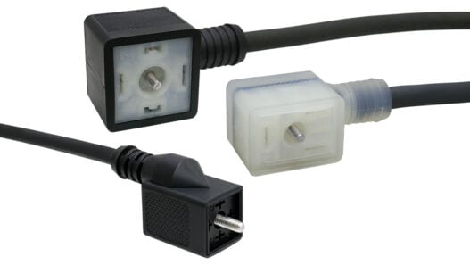
SOICs are commonly used across a range of industries, including consumer electronics, automotive systems, telecommunications infrastructure, and medical devices, particularly where proven reliability, ease of assembly, and long product lifecycles are required.
The term “small outline” refers to packaging standards defined by industry bodies such as the Joint Electron Device Engineering Council (JEDEC) and the Japan Electronics and Information Technology Industries Association (JEITA).
JEDEC defines package outlines, body widths, lead pitch, and naming conventions for many SOIC variants, whilst JEITA maintains similar standards, particularly for packages originating from Japanese manufacturers.
It all starts with the right board
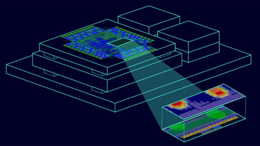
To achieve optimal performance from a SOIC package, careful PCB design is essential. Good layout practices support both electrical and mechanical performance and help to ensure high surface-mount assembly yields. The PCB directly influences the electrical environment in which the IC operates, meaning layout decisions can have a measurable impact on signal integrity, thermal management, and power density.