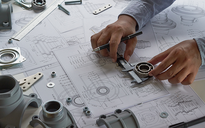
The proficiency in printed circuit board (PCB) design is a distinguishing skill for electrical engineering students. This technical guide delves into the intricacies of PCB layout and fabrication processes, providing a detailed framework for those who wish to master the craft.
Core concepts in PCB design
A robust understanding of PCB components is essential:
- Circuit components: The resistors, capacitors, inductors, ICs, and other elements that constitute the active and passive aspects of the circuit.
- Copper traces: The etched pathways on the PCB that replace traditional wiring, whose width and thickness must be calculated to ensure adequate current flow and to avoid excessive heat buildup.
- PCB substrates: The base material, typically FR4, that provides the mechanical support and the thermal and electrical insulation between conducting layers.
Advanced design principles
High-quality PCB design hinges on adherence to advanced principles:
- Signal integrity: Managing trace impedance and employing techniques like differential pairing to prevent signal degradation.
- Thermal management: Implementing heat sinks, thermal vias, and considering power dissipation in component placement to manage the thermal profile of the PCB.
- EMI considerations: Designing to mitigate electromagnetic interference through careful component placement and trace routing.
Design software proficiency
Competence in industry-standard design tools is non-negotiable:
- CAD tools: Mastery of computer-aided design (CAD) software is necessary for schematic capture and layout design. Popular choices include Altium Designer, Cadence OrCAD, and KiCad for their comprehensive feature sets.
- Simulation software: Tools such as LTspice and PSpice allow for pre-emptive analysis of circuit behaviour under various conditions, crucial for detecting potential issues.
Step-by-step design workflow
The PCB design workflow is intricate and demands meticulous attention:
- Schematic entry: Every design begins with converting the circuit concept into a digital schematic using EDA (Electronic Design Automation) tools.
- Layout design: The schematic is then used to layout the PCB, where considerations of trace length, component placement, and signal paths are vital.
- Routing protocols: Auto-routing can expedite the design process, but manual routing is often necessary for complex signal requirements or specific design constraints.
- Design rule check (DRC): Running a DRC to ensure compliance with electrical standards and manufacturing capabilities is a critical step before finalising the design.
Considerations for manufacturing
The transition from design to production incorporates multiple considerations:
- Gerber files: Generating the industry-standard Gerber files that serve as a blueprint for the manufacturing process.
- Layer stack-up: Strategic layer arrangement to optimise for signal integrity and manufacturability.
- Material choice: Selection of substrate and copper cladding material to meet the specific electrical and thermal performance criteria.
Conclusion
Mastering PCB design is a dynamic and continuous learning process, blending technical knowledge with practical experience. By cultivating a deep understanding of both the theoretical and practical aspects of PCB design, engineering students position themselves at the forefront of innovation in electronics design and manufacture.