


Electric circuits may contain energy storing components, capacitors and inductors. More over, the transistor itself contains capacitances in its structure. Regarding capacitors, let’s consider their time variable constituent: .
A capacitor is characterised with:
memory , so ,
energy storage , so ,
memory , so ,
energy storage , so ,
An electric circuit can also contain components that reflect a magnetic field. So the magnetic field flux and the magnetic flux density is and the total magnetic flux linked to the coil . So the inductor is characterised with:
inductance flux ,
voltage current energy storage, so
inductance flux ,
voltage current energy storage, so
A circuit can also contain transformers and two-terminal devices, consisting of a second coil around the inductor and its small-signal interpretation (Figure 1).
Figure 1.
So the generated voltages for the coils are .
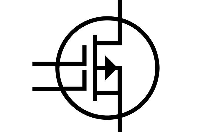
Figure 2 depicts the simplified structure of the n-channel MOSFET.
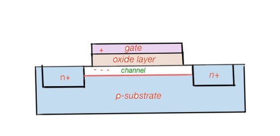
Figure 2. The layer structure of the MOSFET, showing the parasitic gate capacitance.
When positive voltage is applied to the gate, the MOSFET will look like how it is presented in Figure 1, and the layer under the gate will work as a capacitor. Knowing the planar characteristics of a MOSFET, we can calculate its internal capacitor parameters.
A real MOSFET usually contains many capacitors inside. So the gate-source capacitance will be , here . This model also gives us the possibility to use the SRC model of a MOSFET. Here the voltage between the source and the gate will be changed, the current flow will change: , where and are the planar characteristics of the MOSFET internal capacitors. As was mentioned above, real MOSFET behaviour is more complex because of the internal capacitances in the MOSFET structure.
A closer look at the real capacitive structure of the MOSFET is depicted in Figure 3, involving parasitic capacitances.
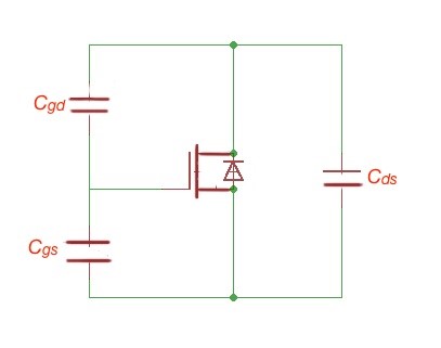
Figure 3. Parasitic capacitance structure of the MOSFET.
The datasheets of different MOSFET manufacturers refer to the , which are input parasitic capacitance, output capacitance and reference capacitance, respectively.
The capacitance is the capacitance showing how much charge is needed for the MOSFET to start to be driven. The is the output capacitance, characterising the turning off time for the MOSFET. The is the reverse capacitance characterising the switching off time for the MOSFET.