


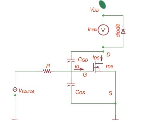
It is very important to understand switching characteristics of power MOSFET. To understand the turn-on and turn–off process in power MOSFETs, we have to consider the simplified equivalent circuits of the power MOSFET in turn-on and turn-off states. When the power MOSFET is off,
,
and
. Let’s first consider turn-on processes among power MOSFET switching characteristics.
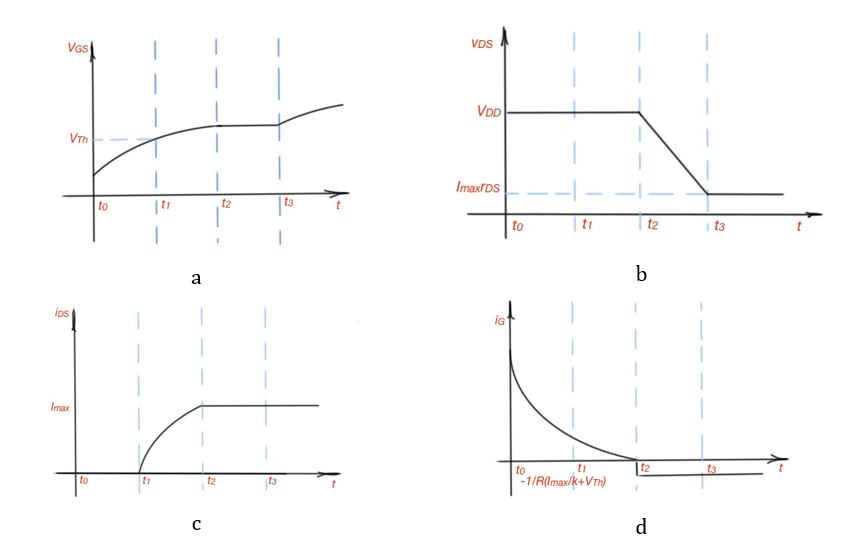
- , when the voltage
is applied, the gate source voltage starts to control the drain-source current, and the capacitor
charges through the resistor
.
- , when the
, the transistor is in the cut-off mode and
This time
is needed to charge capacitor
, and this means delay in time before transistor will turn on. Capacitor
charges to the voltage level
. The gate current
, here
is gate-to-ground voltage, and
is a drain-to-ground voltage. And gate current
Resolving these exponential equations we can show that
, where
, and gate current
,
. Resistance
is characterising conducting state of power MOSFET.
- , then
MOSFET start to conduct current. Delay time
.
- and
, so the
becomes a function of
and
.
- and
,
raises exponentially and is characterised by function
, here is a coefficient, and
,
.
- the drain turns off. Resolving exponential equation we can obtain
.
- , the drain is closed,
. From the equations above
.
- , MOSFET turns off ,
, capacitance
is discharging,
, current flows through
.
- flows through capacitance
,
, gate voltage raises until moment of time
, when gate current
and MOSFET is completely turned off. Time interval
.
- Total delay when power MOSFET is on-state is
, there is a high current and voltage goes through the device during periods of timeand
, that provokes high power losses in MOSFET. Smaller resistance
will decrease power losses.

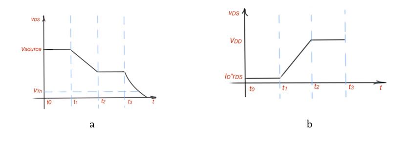
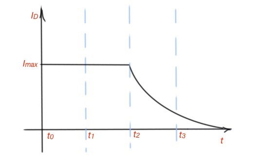
Now we know turn-on part of power MOSFET switching characteristics, so we can consider the turn-off part in the power MOSFET as well. We can assume that the device is on for
.
- When
The equivalent circuit is depicted on figures 2-4. When,
and
are discharging, gate-to-source voltage is
. Current through the capacitor
reaches the constant value
. So
.
- When
, so the current goes through the,
.
- When
, the drain currentbecomes 0, and the service is turned off,
.
- When
the gate voltage continues to fall to 0, and the voltage function is exponential. The gate-to-drain capacitancecharges to the
value.
- When
drain currentdecreases to 0.
The extreme modess of power MOSFETs were explained above. As you can see it is very important to understand every switching characteristics of power MOSFET as MOSFETs are used a lot like switch devices. Let’s briefly consider the Safe Operating Area (SOA). The SOA provides the limits of the power MOSFET to work. Figure 3 depicts the SOA for one of the power MOSFETs from the Infineon product line.
Maximum current is determined by the maximum power dissipation of the MOSFET and follows the formula
and corresponds to the on-state of the power MOSFET. The drain-to-source voltage is growing. The MOSFET starts to work in the saturation mode. Here the device experiences big values of current and voltage. When the drain-to-source voltage grows further the device experiences the avalanche breakdown (it is indicated as the second breakdown limit). Digi-Key Electronics has a great selection power MOSFETs.

(«Power Electronics Handbook», 3rd edition, M.H. Rashid.; «Infineon OptiMOS Power MOSFET datasheet explanation», Infineon Technology AG.)