


Objective
The purpose of this activity is to investigate the common source configuration of a MOS transistor.
Background
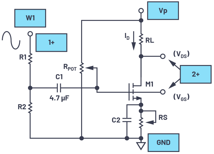
The common source amplifier is one of three basic single-stage amplifier topologies. The MOS version functions as an inverting voltage amplifier. The gate terminal of the transistor serves as the input, the drain is the output, and the source is common to both input and output (it may be tied to the ground reference or the power supply rail), which gives rise to its common name.
Materials
- ADALM2000 active learning module
- Solderless breadboard
- Five resistors
- One 50kΩ variable resistor, potentiometer
- One small signal NMOS transistor (ZVN2110A)
Directions
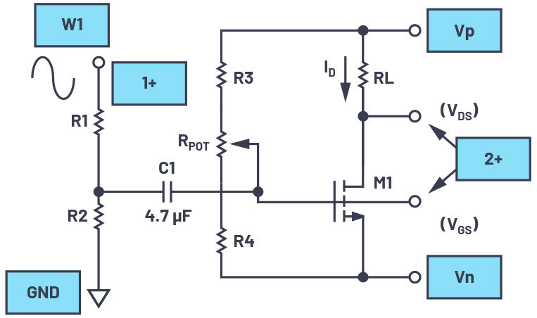
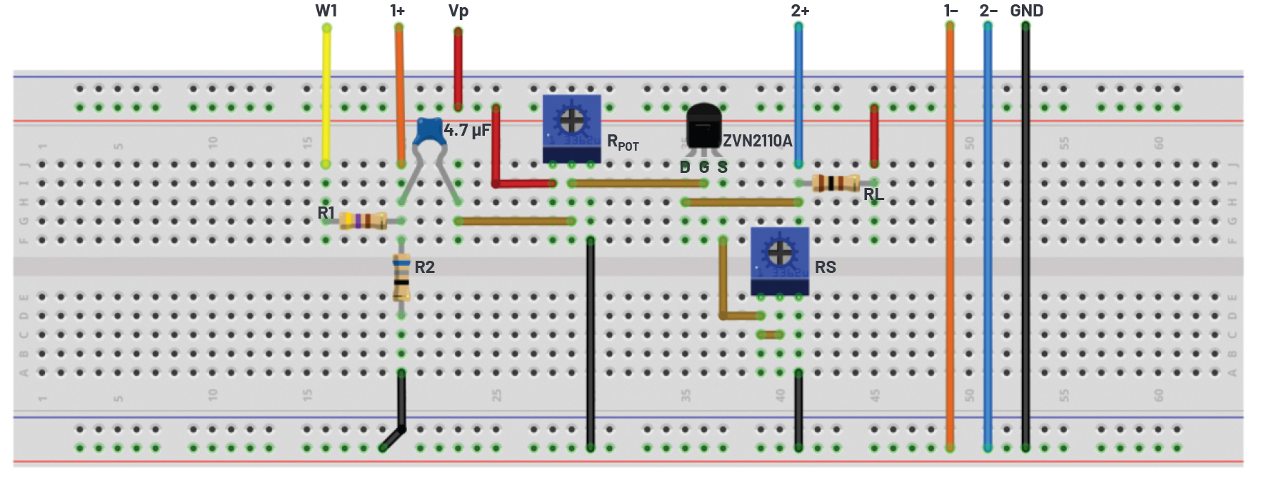
The configuration, shown in Figure 1, demonstrates the NMOS transistor used as the common source amplifier. Output load resistor RL is chosen such that, for the desired nominal drain current ID, the voltage appearing at VDS is approximately halfway between the positive supply voltage VP (+5V) and the negative supply voltage VN (–5V). Adjustable resistor RPOT sets the nominal bias operating point for the transistor (VGS) to set the required ID.
Voltage divider R1/R2 is chosen to provide a sufficiently large attenuation of the input stimulus from waveform generator W1 such that the amplitude of W1 is approximately the same as the signal amplitude seen at VDS. This is done to more easily view the waveform generator W1 signal, given the rather small signal that will appear at the gate of the transistor, VGS. The attenuated W1 signal is ac coupled into the gate of the transistor with 4.7μF C1 so as not to disturb the dc bias condition.
Hardware setup
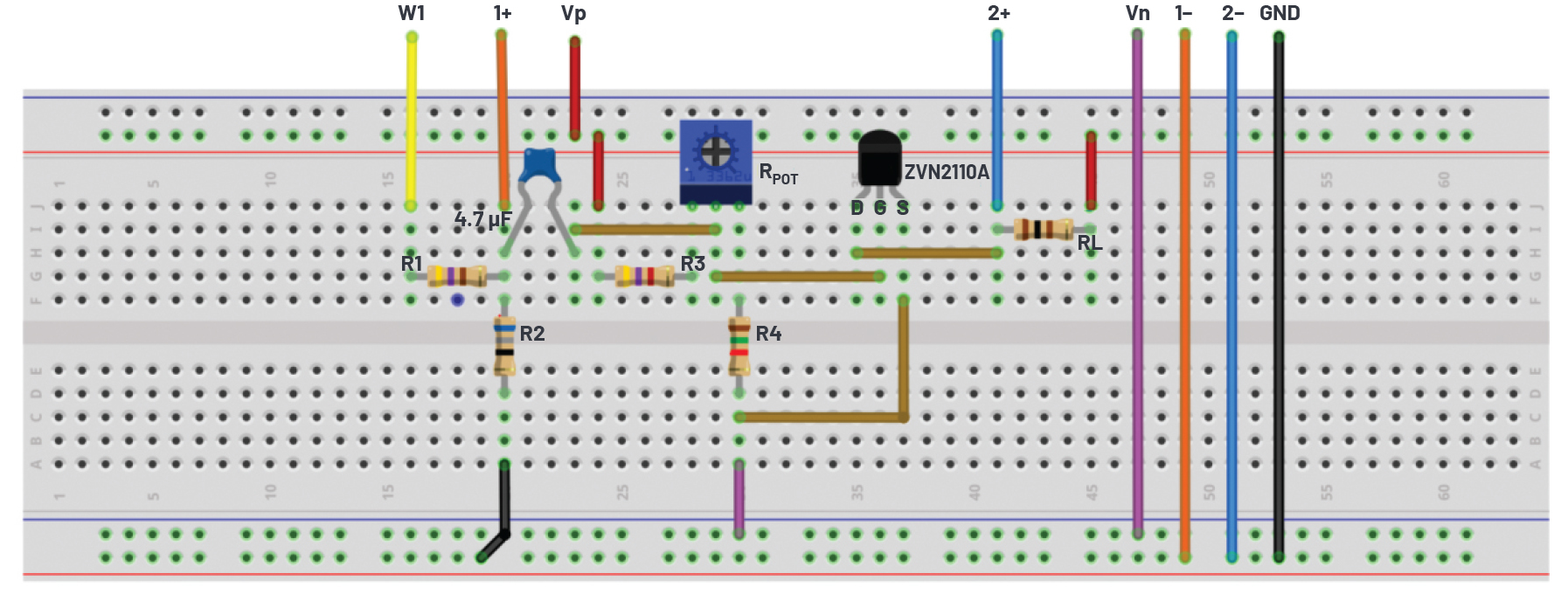
The waveform generator W1 should be configured for a 1kHz sine wave with 3V amplitude peak-to-peak and 0V offset. The setup should be configured with Scope Channel 1+ connected to display the output W1. Scope Channel 2 (2+) is used to measure alternately the waveform at the gate and drain of M1.
Procedure
Turn on the power supplies connected to the drain (VP = +5V) and source (VN = –5V) of the MOS transistor.
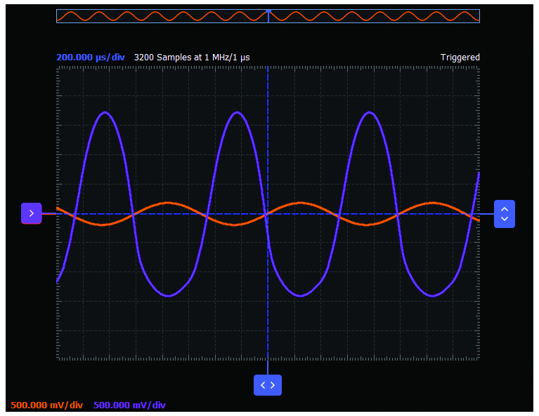
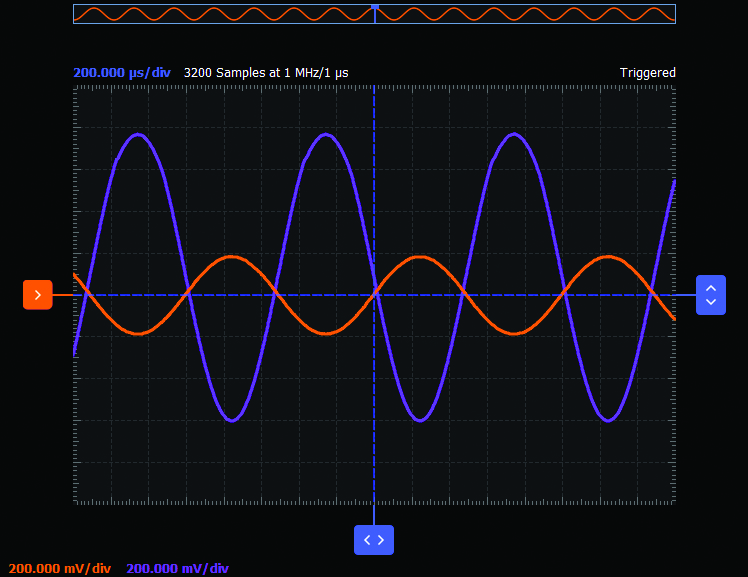
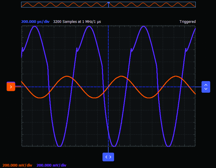
Configure the oscilloscope instrument to capture several periods of the input signal (orange trace) and the output signal (purple trace).
A plot example is presented in Figure 3.
The voltage gain, A, of the common source amplifier can be expressed as the ratio of load resistor RL to the small signal source resistance rs. The transconductance, gm, of the transistor is a function of the drain current ID and the so-called gate overdrive voltage, VGS-Vth, where Vth is the threshold voltage.

The small signal source resistance is 1/gm and can be viewed as being in series with the source. Now with a signal applied to the gate, the same current flows in rs and the drain load RL. Thus, the gain A is given by RL × gm.

Adding source degeneration
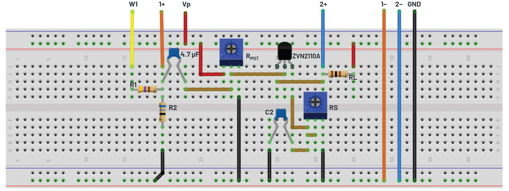
Common source amplifiers give the amplifier an inverted output and can have a very high gain and can vary widely from one transistor to the next. The gain is a strong function of both temperature and bias current, and so the actual gain is somewhat unpredictable. Stability is another problem associated with such high gain circuits due to any unintentional positive feedback that may be present. Other problems associated with the circuit are the low input dynamic range imposed by the small signal limit; there is high distortion if this limit is exceeded and the transistor ceases to behave like its small signal model. When negative feedback is introduced, many of these problems are reduced, resulting in improved performance. There are several ways to introduce feedback in this simple amplifier stage, the easiest and most reliable of which is accomplished by introducing a small value resistor in the source circuit (RS). This is also referred to as series feedback. The amount of feedback is dependent on the relative signal level dropped across this resistor.
The source degeneration gain equation:

Additional materials
One 5kΩ variable resistor, potentiometer
Directions
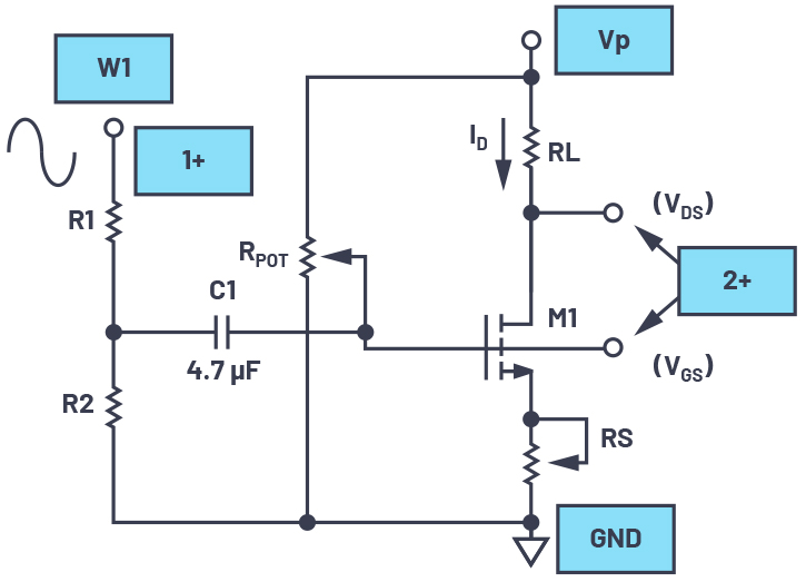
Disconnect the source of M1 from ground and insert RS, a 5kΩ potentiometer, as shown in Figure 4. Adjust RS while noting the output signal seen at the drain of the transistor. The gain of the circuit can be adjusted by modifying the value of the RS potentiometer.
Hardware setup
The waveform generator W1 should be configured for a 1kHz sine wave with 3V amplitude peak-to-peak and 0V offset. The setup should be configured with Scope Channel 1+ connected to display the output W1. Scope Channel 2 (2+) is used to alternately measure the waveform at the gate and drain of M1.
Procedure
Turn on the power supplies connected to the drain (VP = 5V).
Configure the oscilloscope instrument to capture several periods of the input signal (orange trace) and the output signal (purple trace).
A plot example is presented in Figure 6.
Increasing the AC Gain of a Source Degenerated Amplifier
Adding the source degeneration resistor has improved the stability of the dc operating point at the cost decreased amplifier gain. A higher gain for ac signals can be restored to some extent by adding capacitor C2 across the degeneration resistor RS, as shown in Figure 7.
Hardware setup
The waveform generator W1 should be configured for a 1kHz sine wave with 3V amplitude peak-to-peak and 0V offset. The setup should be configured with Scope Channel 1+ connected to display the output W1. Scope Channel 2 (2+) is used to measure alternately the waveform at the gate and drain of M1.
Procedure
Turn on the power supplies connected to the drain (VP = 5V).
Configure the oscilloscope instrument to capture several periods of the input signal (orange trace) and the output signal (purple trace).
A plot example is presented in Figure 9.
Questions
How does adding negative feedback help to stabilise the dc operating point?
For the source degeneration circuit setup, what is the effect on the voltage gain, A, by increasing RS?
You can find the answers at the StudentZone blog.
By Doug Mercer, Consulting Fellow, and Antoniu Miclaus, System Applications Engineer, Analog Devices.