


As lighting plays a major role in interior design and comfort, consumers often make LED lighting the first steps they make when beginning their smart home journey. With support for wireless communications, remote control over light intensity and colour makes the LED an ideal choice for setting different moods and comfort levels.
Buying and fitting wireless-controlled LED lamps provides a boost to smart home market growth. LED lamps readily support the simplest of home networks, where a smartphone or similar device acts as a host. There is no need to install a separate network hub. However, currently, only around 10% of the LED bulbs installed have connectivity. This provides a major opportunity for vendors, with plenty of room to grow in a market where LED lighting sales are growing 20% each year. The key is to minimise production and assembly costs and, with that, deliver lower purchase prices to consumers.
That lower cost must come without sacrificing the levels of quality or reliability that are important to delivering on LED lighting’s promise of greater longevity and operational reliability once installed. There are several key constraints on LED lighting designs. In most cases, these devices need to fit into a strictly defined and compact form factor. The operating conditions are also challenging from an RF perspective. The design needs to maximise wireless transmission and reception range while penetrating walls and tackle interference from Wi-Fi and other networks that use the same frequency range while meeting strict emission levels themselves outside the target spectrum.
The RF and control circuitry need to operate reliably over a wide temperature range in an enclosure next to hot LED and power-supply components. And safe operation is a prerequisite. The power supply to the LED array and any control circuitry will be direct from a high-voltage mains source.
Against those requirements is the need to keep costs low, which places a focus not just on the bill of materials (BoM) but on the type of PCB on which they are mounted. In older LED lamp designs that do not offer wireless control and connectivity, there will be two PCBs. The high-power LEDs will sit on a metal-core PCB while driver circuitry resides on a separate conventional FR4 board. Such a dual-board design increases BoM and assembly costs, which is why manufacturers began moving to a driver-on-board implementation based on a single, combined PCB.
Smart bulb designs can now look at a similar transition. With today’s high-performance connected LED-lamp designs, there will be a metal-core PCB dedicated to the LED elements with a separate control board that contains an additional AC/DC converter that feeds power to a wireless module for connectivity. Such modules ease design because they often integrate antennas and are supplied with regulatory pre-certification for the RF circuitry. But all this comes at a cost that designers can avoid by leveraging driver-on-board construction.
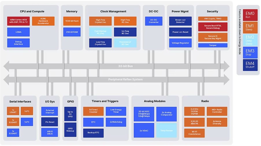
Silicon Labs has performed research on how to build a high-integration LEDand-wireless module that can deliver the low cost associated with driver-on-board designs. An important first step is to use a system-on-chip (SoC) with a microcontroller core to handle both system functions and wireless connectivity. A suitable choice is the Silicon Labs EFR32MG24 (Fig. 1). This SoC not only implements wireless connectivity, but can also directly control a linear LED driver circuit, omitting a dedicated LED driver IC.
That leaves just the LEDs, driver transistors, and power conversion to fill in the rest of the BoM. In terms of space required, a single PCB is a workable option.
The key to making such a design work is to take advantage of electromagnetic simulation tools to create an RF design that is compatible with the LED circuitry and a single-layer, metal-core PCB. As its name suggests, the core of this type of PCB is made from aluminium or copper rather than the fibreglass laminate found in conventional FR4 boards. Above the metal core, there is a thin dielectric layer that may be just 0.1mm thick. Interconnections between components are typically implemented on a single signal layer on top of this dielectric. Though it is possible to form plated through holes to the underside, this adds cost, and so these connections should be minimised where possible. With just one signal layer, compact routing is hard to achieve, which is one reason many designs need to use more than one PCB.
However, a design approach based on careful simulation and experimentation makes it possible to exploit a carrier technology that cannot provide a direct ground reference to the circuitry sitting above it and which, in addition, potentially introduces a high parasitic capacitance. Another key to using a metal-core PCB for more complex electronics is careful component selection. Where a traditional PCB layout will just use vias to let signal lines cross over each other, one under-appreciated option is to use passive components such as surface-mount resistors. A 0402 package, for example, has the external insulation and necessary size to provide an effective way of bridging traces on a single-layer PCB.
Bypass capacitors provide the means to enable filtering of specific frequencies. Placed at critical points, the capacitors are key components of resonant filters that suppress emissions at harmonic frequencies evaluated either using simulation or near-field scanning of a prototype.
The SoC itself can provide the means to control electrical behaviour on the PCB. If there are unused general-purpose I/O pins, they can be shorted in combination with an exposed ground pad. This pad becomes the centre of a star-routed network that helps reduce the formation of ground loops and improves noise rejection.
Because there is no dedicated low-impedance ground layer, the layout requires a low-impedance return path for high-frequency ground currents. The only option is the outer layer. Copper pours and wide traces can deliver the required low-impedance paths and can help couple the metal core to ground.
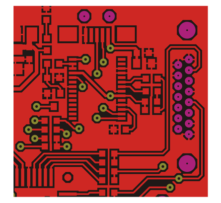
How the metal core couples to ground will affect how the antenna needs to be designed. The metal core brings the advantage of increasing the effective ground area, resulting in a larger antenna area and, with it, improved performance. The rest of the antenna needs to be elevated above the PCB to avoid the metal-core section from acting as a shield. That means a PCB-trace antenna will not work. Some low-cost options for the raised antenna include a helix antenna based on a coil spring, a stamped metal structure or a wire incorporated into the housing (Fig. 3).
Parasitic capacitance is a potential issue. However, engineers can tune this to deliver good performance. In combination with the antenna impedance, the parasitic capacitance of the connection to the PCB pad forms a parallel RLC resonator that acts like a bandpass filter. The right component values will achieve a target frequency, which will typically be 2.4GHz for home automation networks.
Because of these dependencies of the design on PCB and the antenna structure, simulation is an important tool. The tool helps tune the matching and filtering networks, as well as checking the current distribution for the high-power elements. Component models need careful treatment. The models supplied by vendors will often be referenced to a type of ground plane that is not available in this kind of layout. As space is often highly constrained in these designs, some of the larger power-handling components, such as inductors and capacitors, need to be placed under the PCB. Through-hole leads can connect to the opposite side signal layer by a via adapter. In some areas, the distance between high-voltage traces is smaller than what is generally recommended. For this reason, applying conformal coating or potting may be necessary.
As technology progresses, the decreasing trend in SoC power consumption will help reduce the output requirements for the power supply, ultimately reducing the overall component footprint. PCB manufacturing technology is also advancing, which may provide new opportunities for component placement in cost-effective ways.
As the demand for home automation at low cost continues, innovative design approaches will help LED lighting manufacturers, among others, capitalise on this fast-growing market. The design work that suppliers such as Silicon Labs are performing will provide manufacturers with a path to improved solutions.

By Marton Komancsik, Applications Engineer, Silicon Labs
This article originally appeared in the August’25 magazine issue of Electronic Specifier Design – see ES’s Magazine Archives for more featured publications.