
Multi-level cell technology is making Flash memory even more prolific
The use of Flash memory is ubiquitous, but the introduction of multi-level cell technology could make it even more prolific.
By Ethan Chen & Precyan Lee, Advantech.
Flash memory devices employing either NAND and NOR technology are often compared side-by-side in terms of data storing, but to highlight their differences one could think that NOR Flash is used for code storage whereas NAND Flash is used for file storage. The reason for this differentiation is because NOR Flash is capable of achieving fast random access and performing fast read operations, but is restricted by slower write and erase operations. Therefore, NOR Flash is more suitable for infrequent data modification, and it is common to see that boot code, firmware or operating system to be stored in NOR Flash.
On the other hand, NAND Flash is capable of performing fast write and erase operations. It also consumes less layout area, which could be translated to greater density and lower cost-per-bit. Almost as good as it sounds, NAND Flash has one thing that is unable to outperform NOR Flash; slower random access is the trade off for space saving. Nevertheless, NAND Flash is still widely used in various types of file storage elements such as USB Flash drives and memory cards, where data constantly needs to be loaded and updated.
 and for NAND (right)..jpg)
Figure 1 - Cell Array for NOR (left) and for NAND (right)
Figure 1 represents the physical differences between NOR and NAND Flash. The NOR structure (Left) is designed to connect each memory cell (highlighted in yellow) vertically, whereas the NAND structure (Right) is designed to connect each memory cell (highlighted in yellow) horizontally. 10F2 and 4F2 represent the layout area per cell for NOR and NAND, respectively. As mentioned before, NAND Flash requires less layout-area consumption and therefore delivers a wider range of capacities and lower bit-cost.
Know your NAND
Generally, NAND Flash is categorised in two types – SLC and MLC. NAND-makers have recently announced the latest Flash technology - TLC (Ternary-Level Cell), also known as three-bit per cell, which is the new addition to the NAND family. However, it is beyond the scope of our topic and will not be covered in this article.
 and MLC Flash (right), respectively..jpg)
Figure 2 - Cell distribution vs. Threshold voltage for SLC Flash (left) and MLC Flash (right), respectively
Each cell comprises a single transistor and a floating gate, which is located between Gate and Source/Drain and allows electrons to be stored inside. For SLC Flash, only one bit could be stored to each cell at a time, and there will be two possible states for each cell - 0 or 1. As for MLC Flash, two bits could be stored to each cell at a time and there will be four possible states for each cell – 00, 01, 10 or 11. Cell state is determined by the threshold voltage (Vt) of each cell, and the voltage is an interpretation of the amount of charges stored inside the floating gate, as shown in Figure 2.
Because MLC Flash stores more bits it provides higher density and lower bit-cost. Unfortunately, nothing comes for free - the trade-off for cost-saving is greater power consumption and poorer endurance, due to more voltage levels required and technology limitation. It is common to see SLC Flash used in industrial applications, whereas MLC Flash is used in commercial applications. Although SLC Flash is more durable and provides better performance than MLC Flash, cost is still an issue to users. But could Ultra MLC offer the best of both worlds; greater performance and endurance in an economical solution?
, Ultra MLC (middle) and SLC (right), respectively..jpg)
Table 1 - Cell content for MLC (left), Ultra MLC (middle) and SLC (right), respectively
Ultra MLC consists of a number of fast and slow pages, where only fast pages will be used for programming; it can be thought of as an extended version of MLC Flash. Table 1 explains the concept of Ultra MLC; the first and second bit of a memory cell correspond to a fast and slow page, respectively, as shown in Table 1 (left). Since we program fast pages with Ultra MLC, only the bits highlighted in red in Table 2 (middle) will be used.
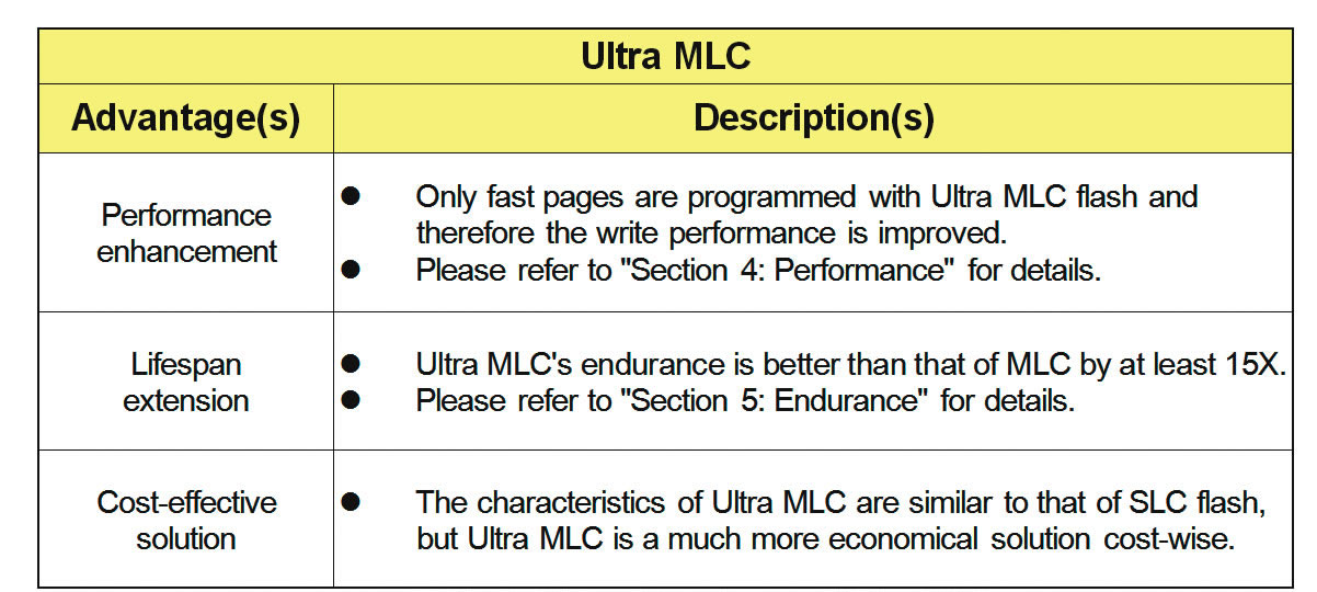
Table 2 - Major advantages of Ultra MLC
When the two bit-sets (10 and 00) from MLC Flash are discarded, the bit data from Ultra MLC is almost identical to that with SLC Flash. The threshold voltage ranges that correspond to 10 and 00 will be discarded, leaving the ones for 11 and 01. Differentiating the amount of charges inside the floating gate becomes easier, since a more separate cell distribution reduces the chance to misjudge the threshold voltage for each cell.
Endurance
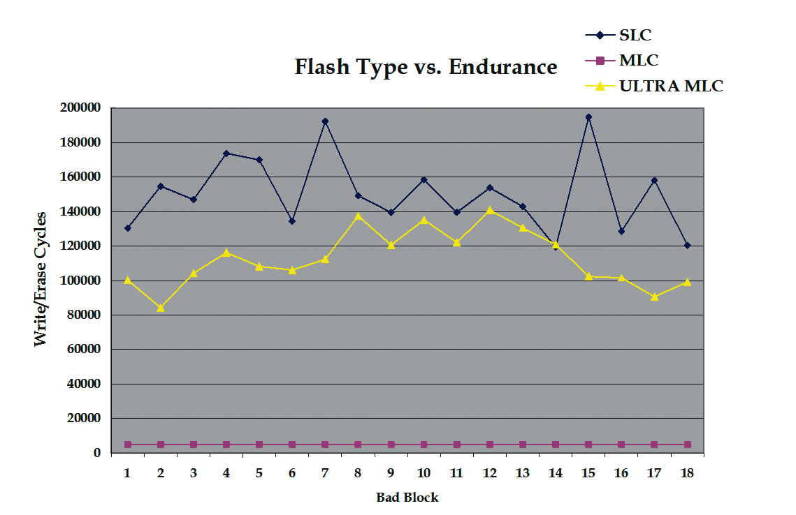
In Figure 3, it is obvious to see that Ultra MLC outperforms MLC in terms of withstanding a greater amount of usage. In general, MLC endurance is considered to be about 3,000 times, and our previous experiments have allowed us to conclude that endurance of Ultra MLC is at least 10 times greater than that of MLC. Since MLC consists of four voltage levels, the chance of one bit influencing the other becomes greater, which could be translated into a higher ECC value. Therefore with MLC Flash, a controller’s ECC-ability needs to be more robust. Conversely, SLC and Ultra MLC have only two voltage levels and the possibility of bit-interference becomes less, which could be observed from a lower ECC value.
Ultra MLC, a part of the MLC family has been proved to provide better performance and greater endurance by programming only fast pages. Our experiment has shown that the read/write performance is improved. Additionally, endurance of Ultra MLC is at least ten times greater than that of MLC, which is used by programming both fast and slow pages. We believe that Ultra MLC is the most economical alternative for Industrial NAND Flash applications when it comes to stable and cost-efficiency requirements.
Product Spotlight
APV1111GVY
Panasonic

Panasonic PhotoMOS® Photovoltaic MOSFET High-Power Drivers
| SKU: | |
|---|---|
| Stock: | 3490 |
| Cost: | $3.95 |
