
ADC clock input considerations
For optimum performance, an ADC’s sample clock inputs (CLK+ and CLK−) should be driven with a differential signal. This signal is typically AC-coupled to the CLK+ and CLK− pins via a transformer or capacitors. These pins are biased internally and require no additional biasing. By Ian Beavers, Staff Engineer, Analog Devices.
High-speed, high-resolution ADCs are sensitive to the quality of the clock input. To achieve superior SNR in a high-speed ADC, the root mean square (rms) clock jitter must be carefully considered based on the required input frequency. The rms clock jitter can potentially limit the SNR of even the best performing ADC, exacerbated at higher input frequencies. The degradation in SNR at a given input frequency (fA) due only to aperture jitter (tJ) can be calculated by:
SNR = 20 × log10 (2 × π × fA × tJ)
In this equation, the rms aperture jitter represents the root-mean-square of all jitter sources, including the clock input, analogue input signal, and ADC aperture jitter. IF under-sampling applications are particularly sensitive to jitter, as shown in the figure. As the analogue input frequency to the ADC triples using the same rms clock jitter, the SNR decreases by 10dB.
The plot shows the SNR-limited performance at various input frequencies across different rms clock jitter profiles. Notice that as the input frequency increases, a lower rms clock jitter will be needed to achieve the same SNR limit as seen at lower input frequencies. For example, 200fs rms clock jitter limits an ADC’s SNR performance to no better than 70dB at 250MHz, but a 1GHz input signal would need 50fs or better rms clock jitter to achieve the same performance.
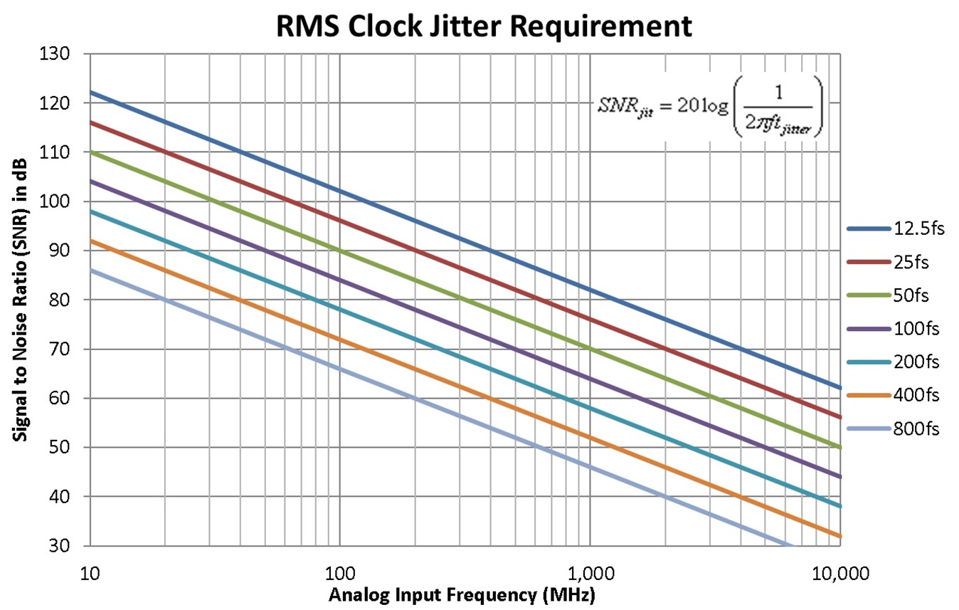
Ideal SNR vs. analogue input frequency and jitter
In cases where aperture jitter may affect the dynamic range of the ADC, treat the clock input as an analogue signal. To avoid modulating the clock signal with digital noise, use separate power supplies for clock drivers and the ADC output drivers. If the clock is generated from another type of source (by gating, dividing, or other methods), it should be retimed by the original clock at the last step.
The two application notes below, 'Aperture Uncertainty and ADC System Performance' and 'Sampled Systems and the Effects of Clock Phase Noise and Jitter', for more information.
 |
Author Profile: Ian Beavers, a staff engineer for the Digital Video Processing Group at Analog Devices (Greensboro, NC), is a team leader for HDMI and other video interface products. With over 15 years’ experience in the semiconductor industry, he has worked for ADI since 1999. He holds a bachelor’s degree in electrical engineering from North Carolina State University and an MBA from the University of North Carolina at Greensboro. |
Product Spotlight
APV1111GVY
Panasonic

Panasonic PhotoMOS® Photovoltaic MOSFET High-Power Drivers
| SKU: | |
|---|---|
| Stock: | 3490 |
| Cost: | $3.95 |
