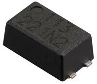
Leadless surface mounted package for CoolMOS MOSFETs
Infineon Technologies announces a new leadless surface mounted (SMD) package for CoolMOS MOSFETs, designated ThinPAK 5x6. With its height of only 1mm and with its very small footprint of 5x6mm, the ThinPAK 5x6 provides 80% volume reduction in comparison to traditional SMD packages such as DPAK.
Chargers for mobile devices, Ultra High Definition TVs and LED lighting all have to meet numerous conflicting requirements. Consumers long for slim yet high performing products. Therefore, manufacturers demand compact, cool and cost efficient semiconductor solutions. These considerable space constraints can be resolved by reducing the size and weight of the components which occupy PCB area.
The worldwide smartphone market, for instance, is expected to grow by 9.4% year over year (2013-2018), according to Strategy Analytics (2014).
For chargers, there is a clear trend towards smaller, faster and more efficient solutions. The very low parasitics of ThinPAK, such as low source inductance compared to the traditional DPAK, reduce the gate oscillation under all load conditions and minimise voltage overshoots during switching by 40% in comparison to traditional SMD thus improving device and system stability and ease of use.
The ThinPAK 5x6 guarantees engineers more flexibility in their PCB designs and better switching performance ultimately leading to more efficient power conversion while reducing overall system size in applications such as low power adapters, lighting and thin panel TVs. It follows the earlier release of the ThinPAK 8x8 which has meanwhile found excellent market adoption in higher power applications such as servers and telecomms SMPS.
Engineering samples of the ThinPAK 5x6 package are available now. Volume production will begin in September 2014.


