
18V buck-boost converter delivers >2A at 95% efficiency
18V buck-boost converter with Intelligent PowerPath control delivers >2A at 95% efficiency from dual inputs.
By Eddy Wells, Design Section Leader, Power Management Products, Linear Technology.
The requirement to operate from multiple input sources is increasingly common for applications powered from various battery chemistries, wall adapters and DC voltage rails such as USB. The ability to provide step-up or step-down conversion is often necessary, depending on the voltage range of each input and the desired output voltage.
While powering from multiple sources is conceptually straightforward, implementation can be complicated. Losses in the power path, prioritisation of the input sources and voltage spikes resulting from inductive cable insertion can all add cost and complexity to the system.
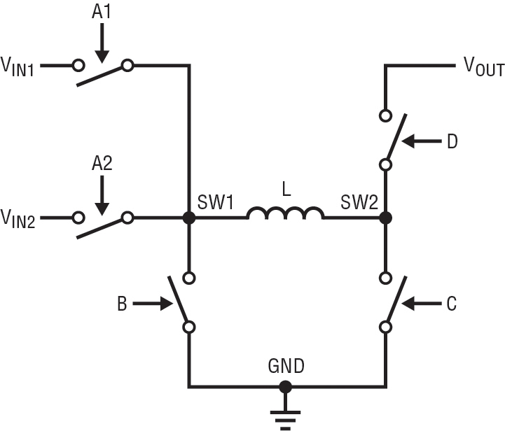
Figure 1 - LTC3118’s dual buck-boost switch
The LTC3118 addresses these issues by combining a dual, low loss PowerPath controller with a high efficiency buck-boost converter, as shown in Figure 1. The unique architecture allows conversion from either input source, VIN1 or VIN2, to a regulated output voltage, VOUT, which can be above or below either input. Operation up to 18V provides sufficient voltage margin for 12V nominal supplies. The converter supports power hungry designs with the ability to deliver over 2A current to the load. The LTC3118’s current mode control architecture responds rapidly to line or load transients, maintaining tight regulation of the output. For battery powered applications, extended run times are achieved with Burst Mode operation.
LTC3118-based designs are flexible, power efficient and small
Multi-input designs are often implemented with external diode-OR circuits. Though low cost and simple, these circuits suffer efficiency losses from the active diode’s forward drop and reverse leakage current in the blocking diode at elevated temperatures. Ideal diode ICs from Linear Technology can be used to improve efficiency and minimise leakage, but are restricted to operating from the higher input source. Highest VIN operation is undesirable if the secondary source is higher voltage than the primary source where energy is more abundant.
The LTC3118 offers operation in “priority” mode, where VOUT is powered from VIN1 (if present and valid) regardless of the voltage at VIN2. Diode-OR operation is still available in “ideal diode” mode, with added hysteresis to prevent chatter when the inputs are equal. As with ideal diode ICs, the forward diode drop is eliminated with the LTC3118’s all N-channel MOSFET design. For flexibility, each input source has an independent UVLO threshold, which should be programmed to set the input’s minimum operating voltage. Additional pins are available to provide the system with VIN and VOUT status, enabling improved monitoring and control.
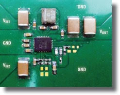
Figure 2 - LTC3118 demo board
The intelligent PowerPath controller plus a single inductor buck-boost converter are integrated in a 4x5mm QFN or 28-pin TSSOP package. The simplicity, flexibility and board area savings of this solution is unrivalled by either an ideal diode or conventional diode-OR power path, followed by a separate buck-boost DC/DC converter. The LTC3118 operates at a fixed 1.2MHz frequency, optimising the trade-off between switching losses and external component size. A complete LTC3118-based system is shown in Figure 2, and is capable of providing over 24W of power in a 400mm2 footprint.
2-cell Li-ion or wall adapter to 12V output with improved switchover performance
Figure 3 shows an application where a 2-cell Li-ion battery is placed on VIN1and a 12V wall adapter is placed on VIN2. In this example, ideal diode mode is selected to force operation from the 12V adapter when present. As shown, high efficiency is achieved over a wide load range from either input source. The battery is placed on VIN1 in this application as VIN1 has lower RDS(ON) MOSFETs and is able to support slightly more load current at low VIN in step-up mode. Maximum load current is limited to 800mA when operating from the low end of the battery’s voltage range at 6V. If needed, the power good indicator /V2GD can be monitored to allow increased load current when the 12V adapter is present.
 LTC3118 schematic; and (b) efficiency curves.jpg)
Figure 3 - (a) LTC3118 schematic; and (b) efficiency curves
Designs with multiple sources often involve “hot plugging” a power source, such as the wall adapter, causing noise and inductive ringing at the input. These transients can be mitigated by reducing the inductance of the cable or increasing the amount of capacitance and/or resistance at the input terminals, but this is impractical in some systems. A LTC3118-based design is better able to manage these transitions and transients in several ways. The wide 2.5 to 18V input voltage range is tolerant of inductive cable ringing in both the positive and negative directions. Separate RUN1 and RUN2 pins allow custom UVLO levels to be set for each input, as shown in Figure 3.
 Wall adapter plugged in; and (b) wall adapter unplugged.jpg)
Figure 4 - (a) Wall adapter plugged in; and (b) wall adapter unplugged
Figure 4a shows a hot-plug event where an inductive cable is inserted on VIN2 in ideal diode mode. As shown, the 12V wall adapter overshoots to 17V due to the inductance of a long cable. Figure 4b shows the response when the cable is unplugged. As shown, the LTC3118 operates from VIN2 until its UVLO engages around 9V and operation from VIN1 resumes. In both cases the average current loop commands the necessary inductor current rapidly, resulting in minimal transients at the output with a 100µF capacitor.
USB/system power or 3 Li-ion cells in Priority Mode with Burst enabled to improve battery life
A second LTC3118-based application is shown in Figure 5. In this example, the 3-cell Li-ion battery stack is placed on VIN2, where VIN1 is used for the USB input. Since operation from the lower voltage USB input should be favoured when available, the LTC3118 is set to VIN1 Priority mode. When operating from the USB, VIN1 and VOUT will be similar in voltage. At the boundary between step-up and step-down modes, the LTC3118’s internal PWM circuit seamlessly transitions, resulting in minimal inductor and output voltage jitter.
 LTC3118 schematic; and (b) efficiency curves.jpg)
Figure 5 - (a) LTC3118 schematic; and (b) efficiency curves
Burst Mode operation provides improved efficiency at light load from either source, as shown in Figure 5b. While light load efficiency is clearly important for the battery input, the USB input may benefit as well if powered from another portable device. The LTC3118’s average current mode control provides excellent load step response, even in Burst Mode operation. Figure 6a shows the transition from a 100mA load where the part operates in Burst Mode, to a 600mA load step where the LTC3118 enters PWM mode quickly, minimising the VOUT transient. Note that USB 3.0 supports up to 1.5A for charging, but is restricted to 900mA during data transfer, the proposed USB 3.1 standard supports up to 2A.
 Load step performance in Burst Mode operation; and (b) Maximum load current for 5VOUT and 12VOUT.jpg)
Figure 6 - (a) Load step performance in Burst Mode operation; and (b) Maximum load current for 5VOUT and 12VOUT
Since the LTC3118 has a fixed inductor current limit of 3A (minimum), the maximum amount of load current that can be supported in (or approaching) step-up mode is reduced with VIN as shown in Figure 6b for both 5V and 12V outputs. This is an important consideration when determining the input source voltages as they relate to the required output voltage and power budget for the load. If the LTC3118’s VCC supply is back-fed from the 5V output as shown in Figure 5a, maximum load current at low input voltages can be improved, as shown in Figure 6b.
Backup system
Figure 7 shows a backup power system where the primary power source on VIN1 is supplied by a 12V system rail or lead acid battery. A 10mF capacitor reservoir on VIN2 is charged up to 18V from a separate supply not shown. In the event the priority VIN1 supply is interrupted, the /V1GD indicator transitions high to alert the system, and the LTC3118 commences operation from VIN2 to keep VOUT in regulation.
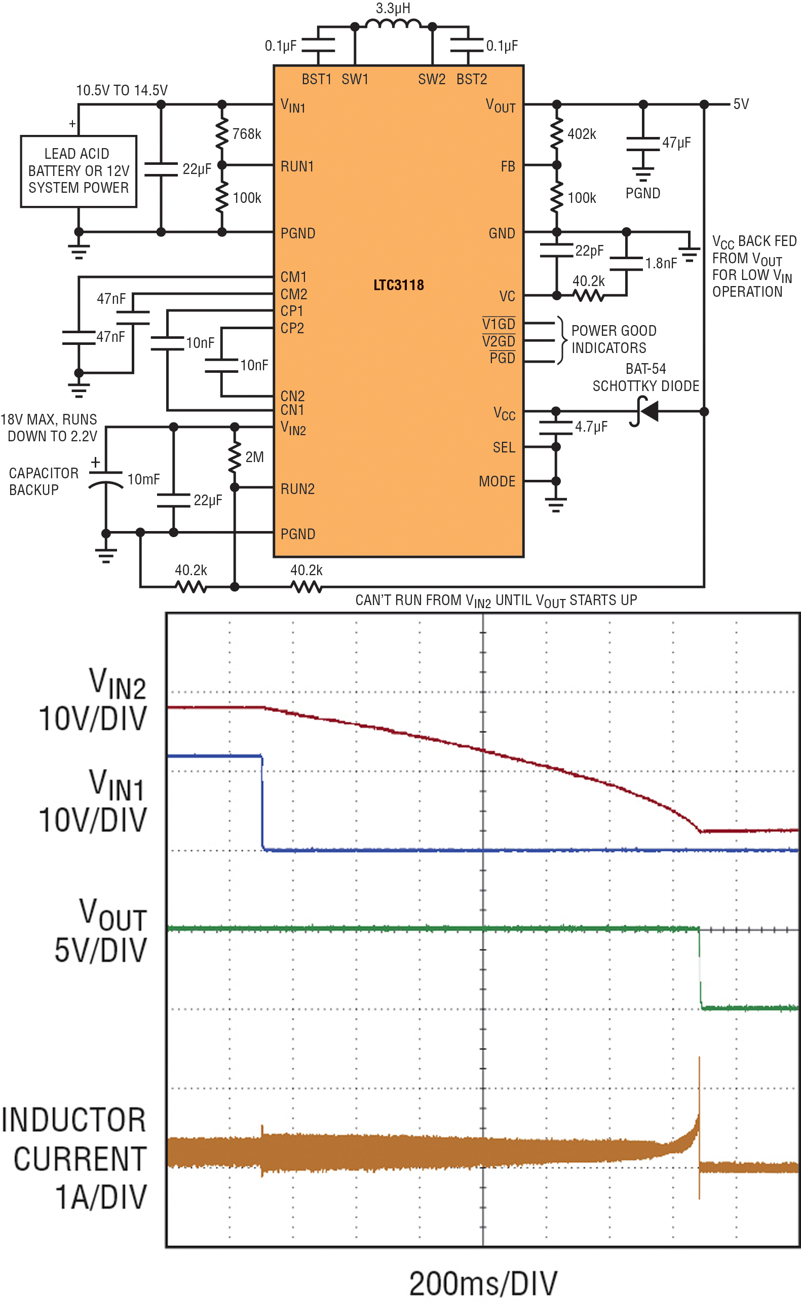
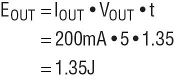
Figure 7 - Backup system holds up system for more than one second to allow for data storage
A scope photo of the backup event is shown in Figure 7, where a 200mA load is supported for over a second to allow a controlled shutdown. Available energy at the input is given by:

In this case, a constant 200mA load is drawn from the LTC3118 as the VIN capacitors are depleted in 1.35 seconds. Output energy is 1.35 joules resulting in an average conversion efficiency of 84% including the supercapacitor losses.
VCC is back fed from VOUT, allowing VIN2 to operate down to 2.2V during the event. The RUN2 pin is connected between VIN2 and VOUT in this case, requiring system power on VIN1 to initially start-up VOUT and ensure clean shutdown behaviour as VIN2 decays during the backup event as shown. The storage capacitance and voltage on VIN2 can be easily modified depending on the requirements of the system.
Summary
The LTC3118 combines an intelligent PowerPath controller with a single inductor buck-boost converter, resulting in a compact platform for multi-input designs. The wide input/output voltage range and ability to support 2A of load current in step-down mode provides a robust solution for a wide variety of applications. The LTC3118’s unique switch architecture allows operation from the higher or lower input voltage to a regulated output voltage. The IC contains the necessary control and indicator pins to give the designer maximum system flexibility. Average current mode control provides rapid response for output load steps or input line steps during switchover. With Linear’s latest-gen buck-boost core and Burst Mode operation, both low noise and high efficiency can be achieved.
Product Spotlight
APV1111GVY
Panasonic

Panasonic PhotoMOS® Photovoltaic MOSFET High-Power Drivers
| SKU: | |
|---|---|
| Stock: | 3490 |
| Cost: | $3.95 |
