
Broader range for diverse applications
The proliferation of low-cost FPGAs now enable broader markets to benefit from MIPI DSI Displays and Application Processors. By Ted Marena, Director of Solutions Marketing, Business Development, Partner Solutions & IP, Lattice Semiconductor.
In the 1990s when the PC was the undisputed high volume architecture, engineers working in other sectors realised that if they adopted the same parts for their own applications they could benefit from the lower costs and high reliability afforded to the PC industry. A broad range of embedded designers leveraged this phenomenon and it drove increased value for the end customer. Over the past few years, however, the PC has been surpassed as the high volume platform and today, smart phones and tablets are king of the hill, while the PC is in decline. But just as the previous generation of designer utilised low cost PC components, today’s engineer desires to achieve the same outcome by using components and devices originally developed for smart phones and tablets.
The majority of smart phones and tablets use buses and interfaces that have been defined by the MIPI standards body. For example, the screen display interface is termed DSI (Display Serial Interface) and the image sensor interface is CSI-2 (Camera Serial Interface). The MIPI standards body defines the interconnect between an applications processor and a wide range of peripherals including image sensors, memories, displays, RF components and sensors. Some embedded designers will even want to utilise application processors for the heart of their system. Unfortunately for many designs this is not possible because existing software and other functions that have targeted generations of embedded processors make the costs exorbitant. However these same designs would still like to leverage the other components often found in a smart phone or tablet. The major challenge in doing this is the connection required to bridge mature interfaces to the various MIPI bus standards, such as DSI.
Engineers face an interface challenge when adopting 'main stream' consumer-led technologies
Screen time
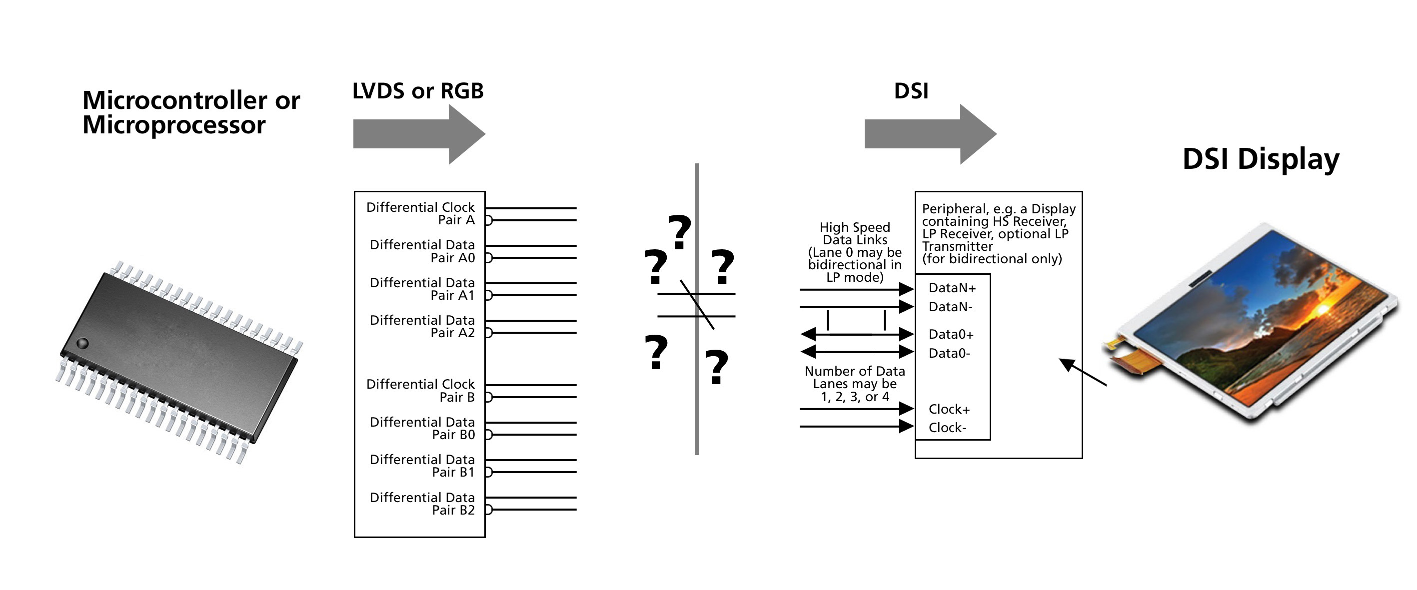
To illustrate, consider a microcontroller that has significant software development and investment; naturally the system designer wants to continue the use of this microcontroller but also wants to integrate a screen found in a mobile device. The DSI interface for the display is a serial SLVS signalling type bus, however the incumbent microcontroller was developed with a CMOS RGB or a LVDS flatlink bus, to connect to an LCD screen. This is incompatible with the DSI interface and thus the two devices will not operate properly.
Not long ago the designer would have had to abandon the idea of using the low cost DSI screen for this embedded design, unless the cost of a bridging ASIC could be justified. For the vast majority of designs this is not the case and another, more expensive display would be required. Fortunately, a low cost, readily configurable solution now exists to address this problem. In fact these and other similar solutions enable nearly any embedded design to utilise low cost DSI screens.
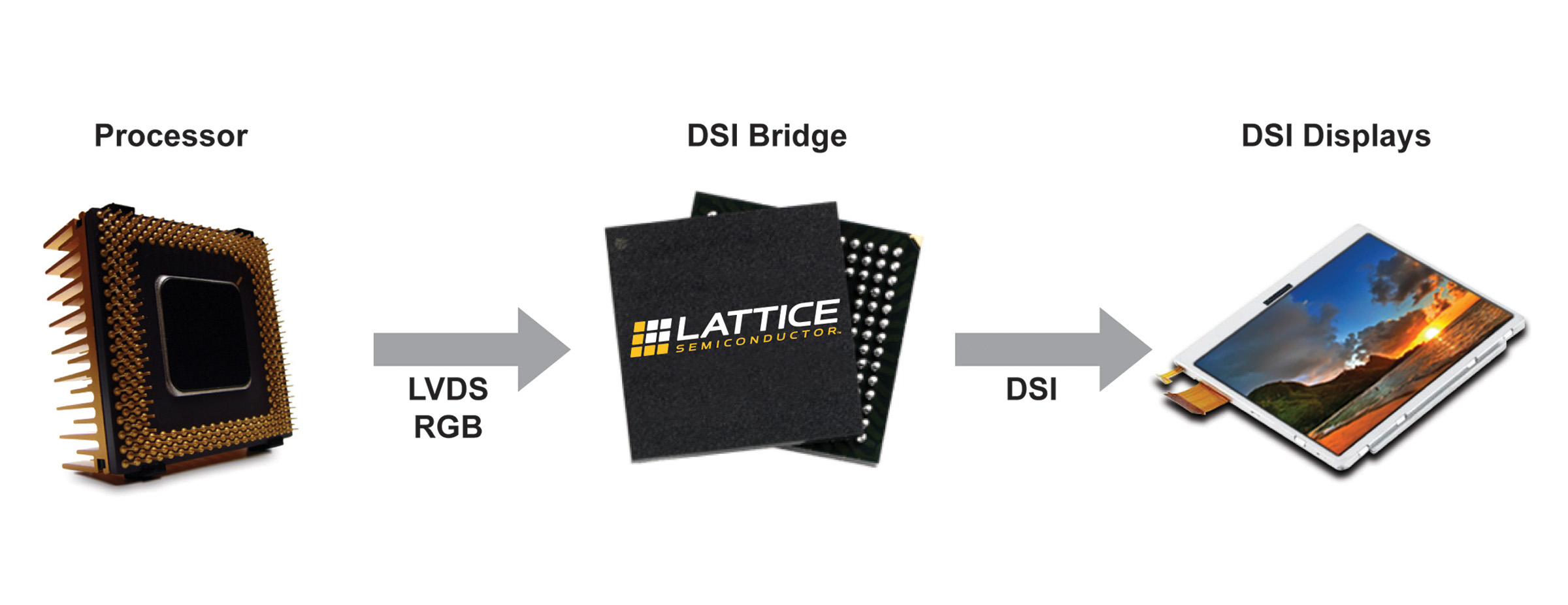
Recently a suite of solutions was released that leverages Ultra Low Density (ULD) FPGAs to bridge to/from MIPI DSI & CSI-2 interfaces to numerous traditional buses. These low cost, low power FPGAs and the MIPI reference designs ported to them provide an ideal bridge chip to connect DSI screens to a wide range of embedded microprocessors or microcontrollers.
As an example, assume the incumbent or preferred microcontroller has a CMOS RGB888 (24 bit colour bus) display interface. The first step is to determine how to program the configuration registers of the DSI screen. Most likely the microcontroller will configure this via an I2C bus. DSI however does not accept I2C for screen configuration; DSI uses the serial data lane D0 for the Display Command Set (DCS). Therefore, the FPGA needs to convert the I2C commands from the microcontroller to a series of DCS commands to configure the DSI screen. Once the screen is programmed, the FPGA must be configured to receive the RGB888 interface. Assuming the screen resolution for the RGB888 bus is the same as the DSI display, the next step would be to convert the parallel bus to the serial DSI bus. If the resolution between the screen and microcontroller varied, the FPGA could scale the image up or down. In either scenario, it would be necessary to configure the number of output data lanes for the DSI interface. Once this is done the ULD FPGA would output a DSI transmit interface to drive a DSI display.
Low-cost FPGAs and associated IP can provide bridging solutions
Non-standards
Of course, some designs that utilise an applications processor may also target an LCD screen that does not use a DSI standard. While a few application processors have more than one type of screen interface bus, most only utilise the DSI standard, thus the same challenge applies. The applications processor will require its DSI output to interface to an LCD screen that is now likely to feature an LVDS flatlink bus. The same ULD FPGA can be configured for this bridge solution. In this type of design, the DSI would be an input bus to the FPGA and the LVDS display would be driven by the FPGA.
Now that designers can access low cost ULD FPGAs to interface to a DSI and CSI-2 interface, numerous mobile components can be considered for their unique designs. Just as the PC boom assisted many embedded designs to reduced costs using PC components, now the same benefit can be enjoyed using mobile components, such as displays, application processors and image sensors, with the help of ULD FPGAs and the DSI & CSI-2 solutions from Lattice Semiconductor Corporation.
Product Spotlight
APV1111GVY
Panasonic

Panasonic PhotoMOS® Photovoltaic MOSFET High-Power Drivers
| SKU: | |
|---|---|
| Stock: | 3490 |
| Cost: | $3.95 |
