
Nulling bridge sensor offsets
A simple circuit provides an effective solution to the challenge of removing offsets in low signal sensor amplification applications. By Gustavo Castro and Scott Hunt, Application Engineers, Analog Devices.
Instrumentation amplifiers (in-amps) can condition the electrical signals generated by sensors, allowing them to be digitised, stored, or used to control processes. The signal is typically small, so the amplifier may need to be operated at high gain. In addition, the signal may sit on top of a large common-mode voltage, or it may be embedded in a substantial DC offset.
Consider a single-supply bridge amplifier where 3.3V is used to excite the bridge and power the amplifier. The full-scale bridge output is ±15mV, and the offset can be in the ±25mV range. To obtain the desired sensitivity, the amplifier gain needs to be 100, and the input range of the ADC is 0-3.3V. The output of the bridge can be positive or negative, so the output is referenced to mid-supply, or 1.65V. When applying a simple gain of 100, the offset would cause the amplifier output to vary from -0.85 to +4.15V, which exceeds the supply rails.
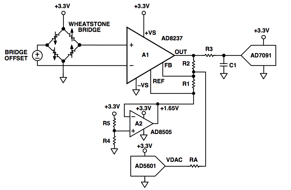
The circuit in Figure 1 solves this problem. Bridge amplifier A1 is the AD8237 indirect current feedback (ICF) in-amp. Amplifier A2, with R4 and R5, sets the zero level output of A1 at mid supply. The AD5601 8-bit DAC adjusts the output to null the bridge offset through RA. The output of the amplifier is then digitised by the AD7091 micropower 12-bit ADC.
Single-supply operation
The DAC can swing ±1.65V around the 1.65V reference voltage (0-3.3V). With VA(MAX) = 1.65V and VIN(MAX) = 0.025V, RA = 65.347kΩ. With 1% resistor tolerance, the closest available value is 64.9kΩ. This leaves no margin for errors caused by source accuracy and temperature variation, however, so choose a low cost, commonly stocked 49.9kΩ resistor. The tradeoff is reduced adjustment resolution, and a slightly larger post-adjustment offset.
With R1 = 1kΩ and R2 = 100kΩ, the nominal gain is 103. If a value closer to the target of 100 is desired, reduce the value of R2 by about 3% to 97.6kΩ to obtain a nominal gain of 100. The total offset adjustment range is given by the voltage divider formed by RA and the parallel combination of R1 and R2, which can be calculated as:
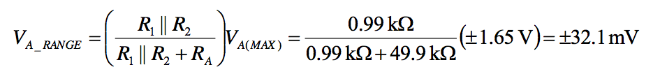
A ±32.1mV adjustment over the ±25mV maximum bridge offset provides an additional 28% adjustment margin. With an 8-bit DAC, the step size for the adjustment is:
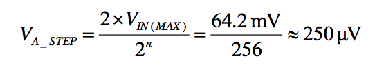
With a 250µV adjustment resolution, the maximum residual offset at the output is 12.5mV. The values of R3 and C1 can be determined from the ADC data sheet. For an AD7091 sampling at 1Msps, these values are 51Ω and 4.7nF. Larger resistor and capacitor combinations can be used when sampling at lower rates to further reduce noise and aliasing effects.
An additional advantage of this circuit is that the bridge offset adjustment can be done at production or installation. If environmental conditions, sensor hysteresis, or long-term drift have an effect on the value of the offset, the circuit can be readjusted. Because of its true rail-to-rail input, the AD8237 works best in bridge applications that employ very low supply voltages. For traditional industrial applications where higher supply voltages are required, the AD8420 is a good alternative. This ICF in-amp operates with supply voltages from 2.7V to 36V and draws 60% less current.
Product Spotlight
APV1111GVY
Panasonic

Panasonic PhotoMOS® Photovoltaic MOSFET High-Power Drivers
| SKU: | |
|---|---|
| Stock: | 3490 |
| Cost: | $3.95 |
