
Creating a negative output voltage using a buck converter
A theory of operation as well as schematics and performance data to enable a the quick implementation of a circuit which require a negative supply and in which only a positive supply is available in the system. By Owain Bryant, Vishay Intertechnology
A synchronous buck regulator offers a simple and efficient method to generate such a supply.
There are some applications, such as double-ended sensors and audio amplifiers that require a negative voltage for operation. A good example of a system needing a negative rail is in the signal path of an instrumentation application. Real-world signals often need to be measured all the way to zero volts, which would not be possible if the operational amplifier measuring the signal is supplied by a positive voltage and ground. Using a positive and negative supply for the operational amplifier allows for the full range of the signal to be measured accurately.
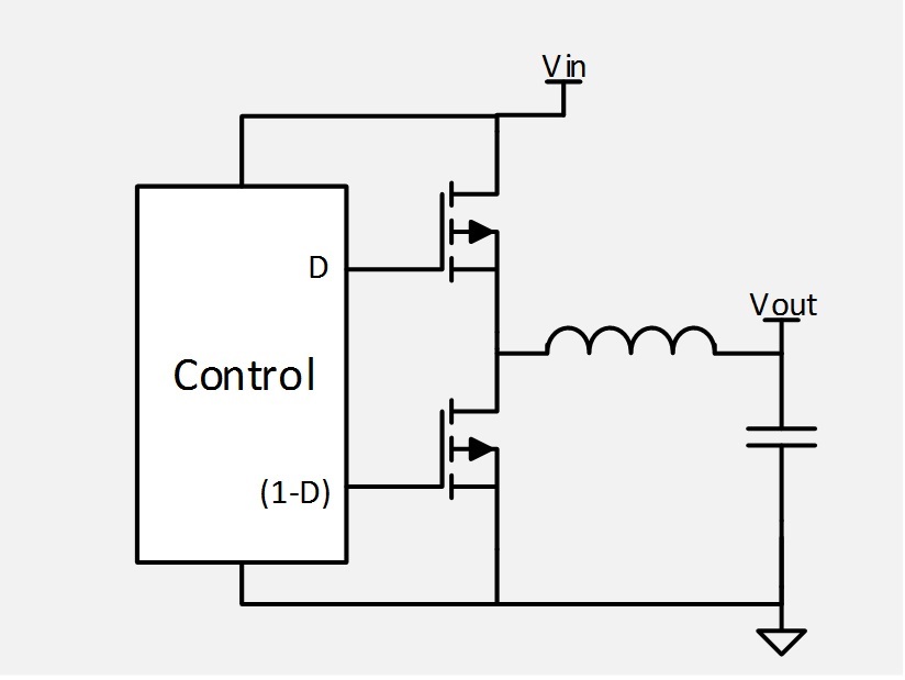
Figure 1: a) Synchronous buck b) Negative output buck
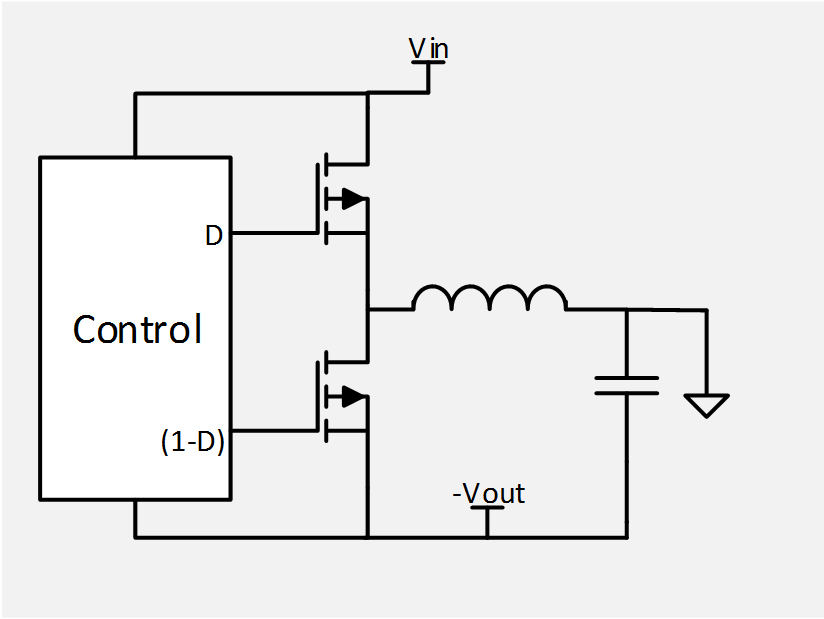
b) Negative output buck
One of the easiest ways of generating a negative voltage is to add an additional winding to an existing transformer-based power supply. However, this may not be possible in a system that does not have access to a transformer in the design. For example, several instrumentation systems are designed to have an external AC adapter that provides a single 12 or 24V DC voltage to the main board. This reduces the size and cost of the system.
In such systems the negative voltage must be generated from an existing positive rail. The synchronous buck regulator suits this application, as it is an efficient topology and today's integrated FET buck regulators use minimal external components.
Generating a negative supply
In order to generate a negative output voltage from a positive input voltage, designers usually opt for the buck-boost topology or possibly a single-ended, primary inductance converter (SEPIC), both of which offer reasonable efficiency that is much higher than a linear regulator. This design idea shows that the same outcome can be reached with a buck converter. With a slight alteration to the nodal references of a synchronous buck converter, we can create a negative boost converter, as shown in Figure 1a and b.
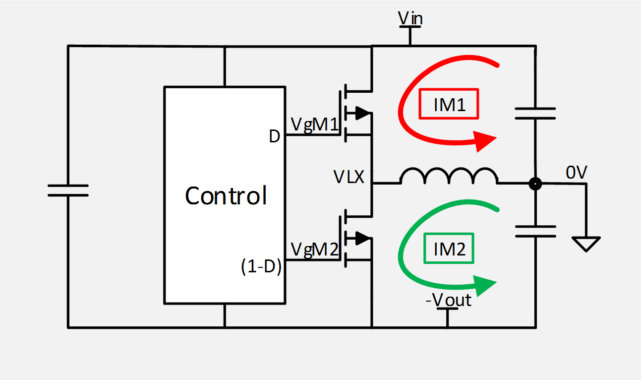 Figure 2: Negative output buck topology
The circuitry in this example is built around the SiP12116 synchronous buck converter. The use of constant on time (COT) topology allows the user to develop a straightforward power supply with no compensation requirements. The buck converter develops the current ramp feedback from the internal low-side metal oxide semiconductor field effect transistor (MOSFET) so the external components required are the power LC filter, input capacitive decoupling, and bootstrap capacitor.
The control of the circuit will be identical to that of the standard buck converter; however, there is a key difference in that the change in nodal connection of the Inductor from Vout to 0V will cause a change in circuit current flow. This in turn allows the negative output voltage to be generated. The IC’s 0V now becomes the negative output voltage.
The MOSFET drive waveforms can be seen Figure 3, which are similar to a standard buck converter. The LX voltage is also shown. LX waveforms range from -3.3 to +12V, and the majority of the magnitude is from -3.3 to 0V when the low-side MOSFET is on. The next trace represents the output voltage -3.3V.
The inductor current can be seen next, which is centred around 0A. There is no load in the simulation. The key waveforms appear next — IM1 and IM2 — which indicate the current flow in the circuit. Note that these waveforms are referenced to 0 V.
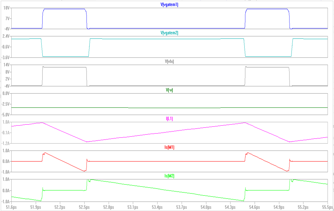 Figure 3: Simulation of nodal waveforms from Figure 2
Current flows from +V to 0V through the high-side MOSFET, but note that the current is flowing from positive to negative, so it is decreasing, as can be seen in the IM1 trace. When M1 is switched off and M2 switched on, the current flows from -V to 0V. This is seen in the increasing current, while MOSFET M2 shows a decreasing current due to the reference point of 0V.
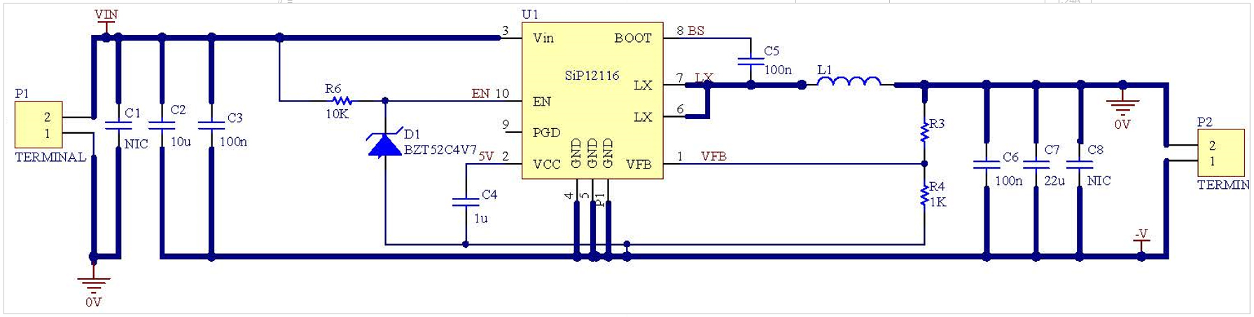 Figure 4: Schematic representing the changes to the nodal reference
The overall design specifications for the circuit are as follows: Vin = 12V, Vout = -3.3V, Fsw= 600khz, Iout = 3A, Vripple = 150mV, and Vin_ripple = 100mV.
The synchronous buck converter senses the current across the low-side MOSFET, so this signal needs to be reasonably large in order to stand out from any system noise that may be present. The method for this is to use a large ripple current, set to 40% of the load current. This will also allow the user to downscale the size of the inductor. It is worth noting at this point that the calculations for the controller are relatively straightforward as the system runs with a COT topology, while also being controlling current internally derived through the low-side MOSFET, leaving few external parts that need design calculations.
The schematic in Figure 3 represents the changes to the nodal reference with Vout becoming 0V and 0V becoming –Vout. One must ensure there is decoupling across the input to 0V, and some decoupling across the input to –Vout.
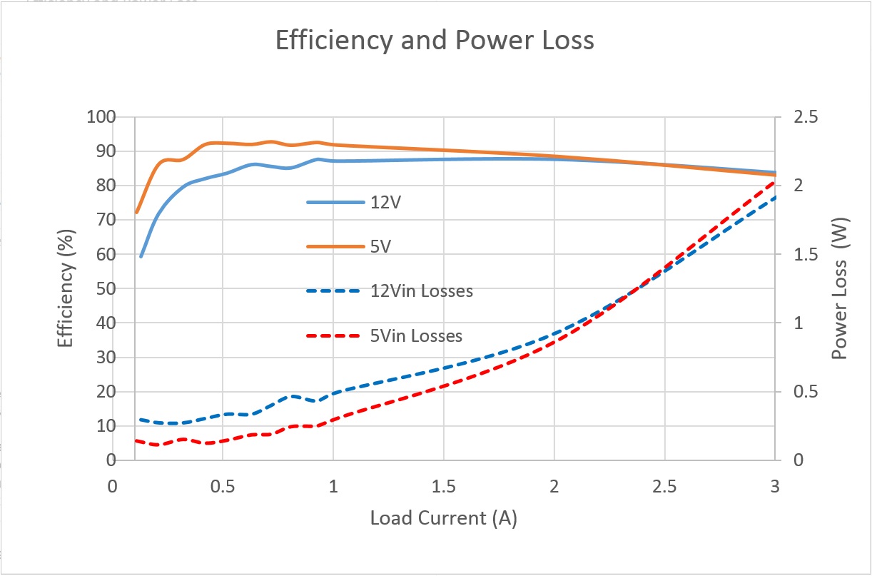
Figure 5: Efficiency measurements at test conditions
As is demonstrated, for applications which require a negative supply and in which only a positive supply is available in the system, a synchronous buck regulator offers a simple and efficient solution. The limit to the range of output voltages that can be generated depends on the device used. For example, the SiP12116 has a maximum operating voltage of 16V. Therefore with a 12V input, it can generate up to -4V output. However with an input voltage of 5V, it can generate a –ve output of up to -11V. In the example presented, a 12V supply is used to generate a -3.3V output at an efficiency of over 90%, and demonstrates both the efficiency and the elegance of using a buck regulator to generate a negative supply voltage.
Product Spotlight
APV1111GVY
Panasonic

Panasonic PhotoMOS® Photovoltaic MOSFET High-Power Drivers
| SKU: | |
|---|---|
| Stock: | 3490 |
| Cost: | $3.95 |
