
Automated Test Equipment in the Cloud
A revolutionary pay-per-use solution combines semiconductor test with cloud computing technology, offering semiconductor companies access to test capabilities while minimising investment and effort. Stephane Cavazzini, Advantest’s Sales Account Manager for SOC IDM, explores further in this ES Design magazine article.
In the semiconductor industry, designers who need to verify a prototype chip or new silicon mostly use dedicated bench equipment to set up a tester and run focused tests. This method is time consuming and expensive due to the effort spent in verifying the setup and the cost to use oscilloscopes, signal generators and analysers. Besides, it creates difficulties to maintain the testing environment across multiple engineering teams and/or sites, which it often necessary to accelerate the silicon/system debug, and verify and assure test quality.
Alternatively, designers might use traditional Automated Test Equipment (ATE) for the same purpose. This means allocating ATE tester time on an as-needed basis while developing chip validation test programs using languages like C++ or Java. However, small organisations cannot always afford the cost of acquiring ATE, and others are reluctant to give up tester time which is invariably in high demand for test engineering, production test program validation and volume production needs.
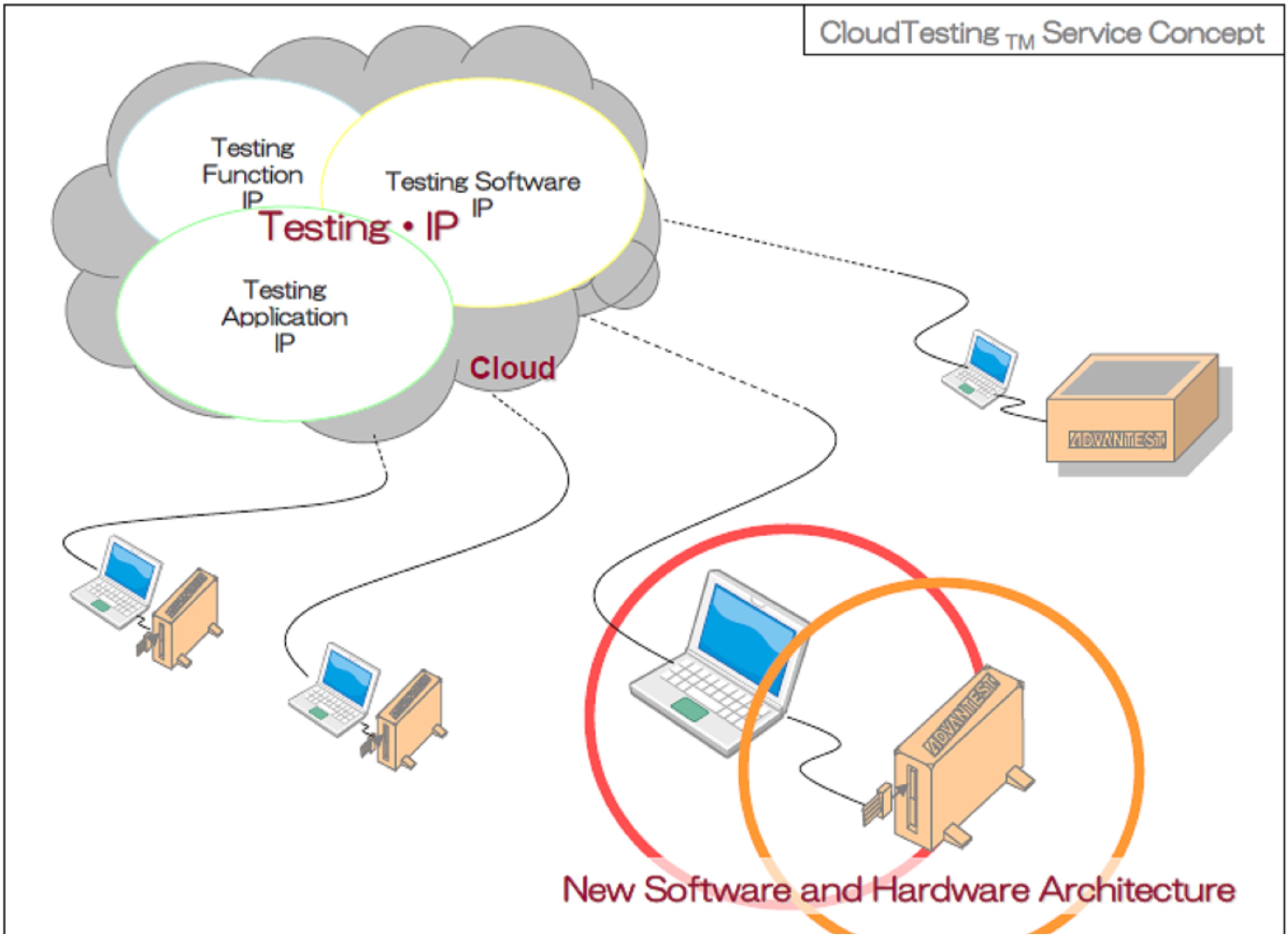
Figure 1: The CloudTesting Service
To resolve this issue the CloudTesting Service (CTS) has been created, which allows users to sign up for a test service intended to replace the need to buy and maintain — or lease — expensive test equipment. The user can download IPs resident in the cloud to test and characterise new silicon. The compact desktop tester used for executing algorithms is provided for the entire duration of the subscribed service, only interfacing cables are required to connect the tester to the device performance board (Figure 1). This one-time, low-cost item can be acquired on the CTS website.
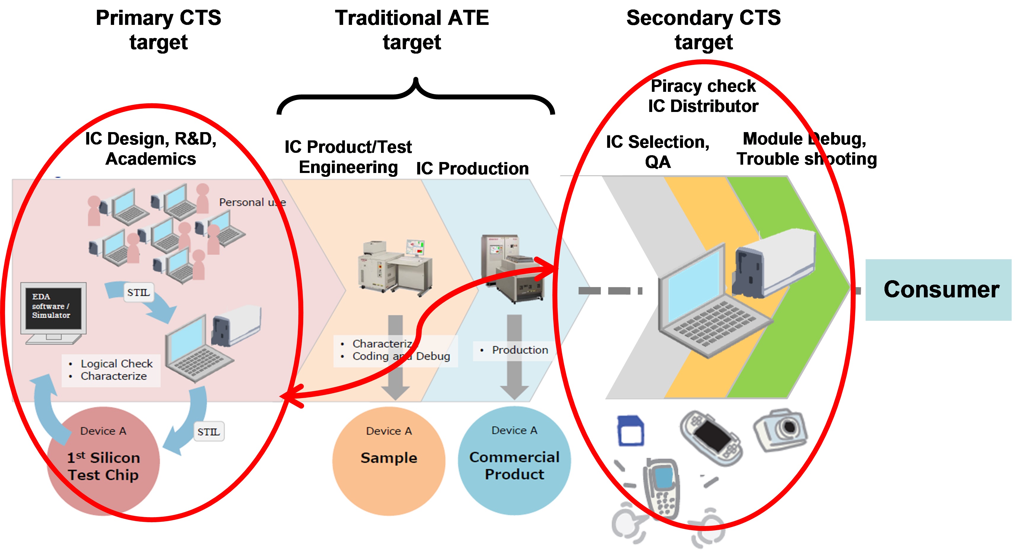
Figure 2: CloudTesting target users
Concept
CTS primarily targets IC designers, R&D teams, academics and research institutes, but its benefits could extend to distributors for IC selection and quality, or returned customer module trouble shooting. This applies to both ends of the IC chain.
The concept allows the user to download a set of tools from the cloud, such as algorithms and testing functions, directly onto a laptop to build individualised test environments using the CTS software interface. Once the test flow is complete, it can be downloaded to the portable CloudTesting Station connected to the Device Under Test.
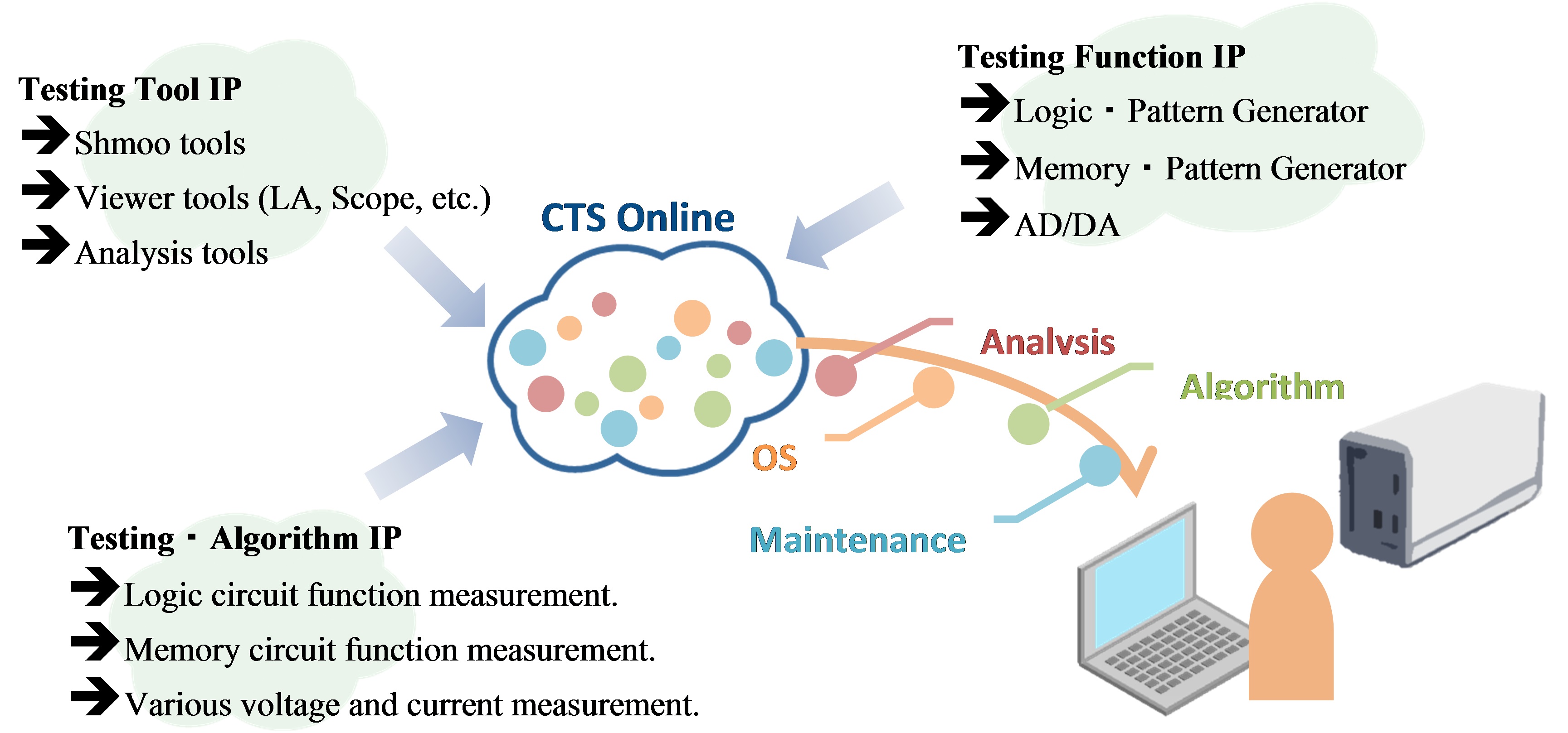
Figure 3: CloudTesting concept
As a first step, the user should connect to the CTS portal site http://cts-advantest.com/en/, which provides a description of the concept, as well as a detailed IP licensing description and selection assistant.
As a second step, the user registers and sets up an account in order to be able to download user manuals, basic software and selected IPs from the e-Commerce web site.
The downloaded CTS intuitive user interface can define the device test environment conditions such as pin definitions, type of measurement or/and functional test required (using selected IPs) with a user’s own setup and execution conditions (power setup, levels, patterns, timing, etc.), as well as flow execution. No specific, dedicated programming language is required. Analysis tools such as pattern viewer, logic analyser, oscilloscope, shmoo tool, etc. are also available through dedicated IPs.
.jpg)
Figure 4: Pattern signal setup of selected functional test (IP)
Test conditions and projects can be imported from CSV files and close loop link to EDA environment is supported through STILReader/Writer IPs (VCD/eVCD IPs are under development).
An example of possible flow definition, including external thermo-streamer control, simulation output data usage for functional testing setup and analysis tool for results interpretation — combined with various voltage, current and frequency measurements and DAC verification — is shown below in Figure 5.
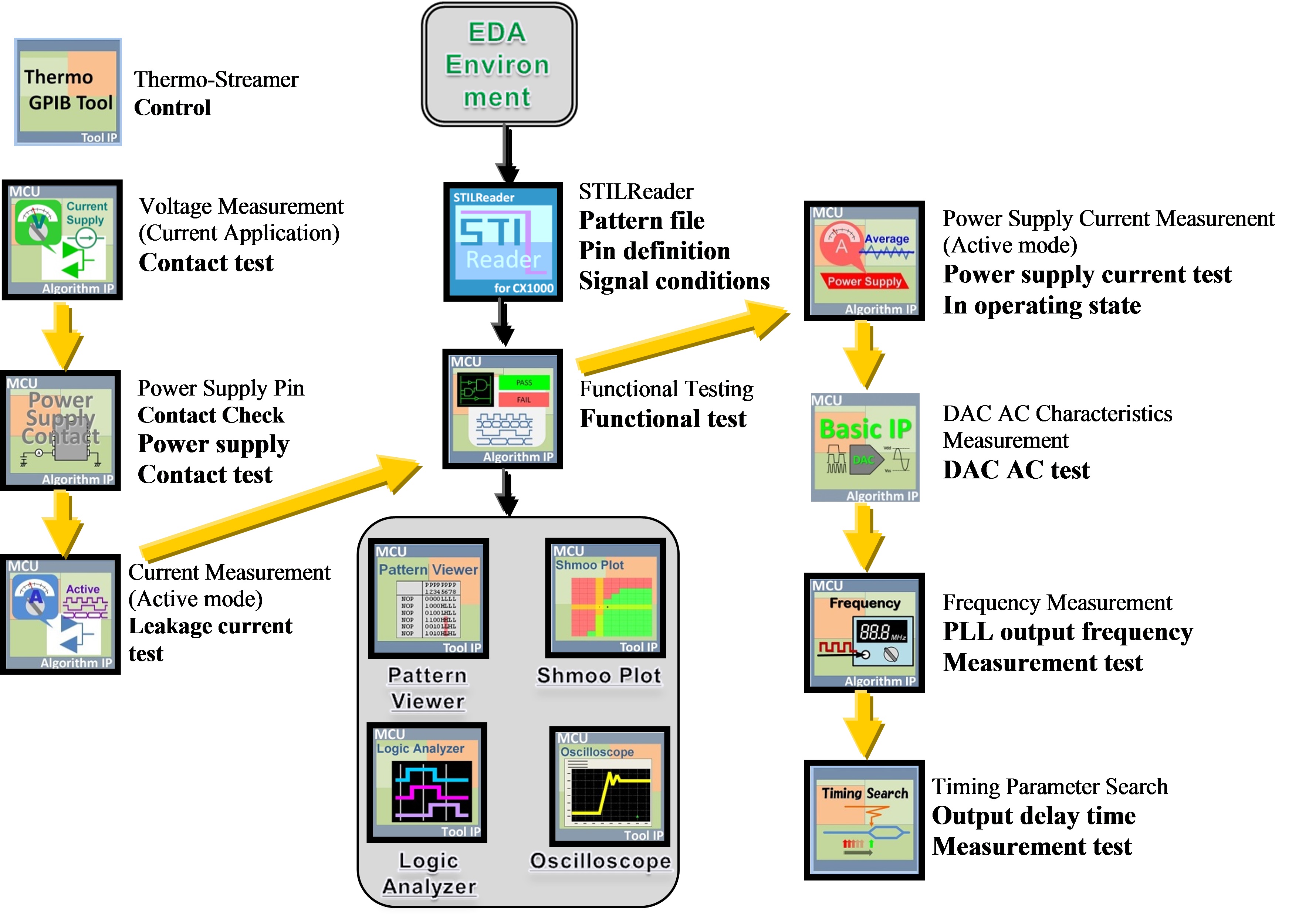
Figure 5: Example of possible flow setup using various IPs
Hardware overview
Two compact testers with three different configurations are available for executing the test algorithms. To operate and control the CloudTesting station only a laptop with Windows7 64-bit is required; CTLab software needs to be installed and required IPs have to be downloaded.
The test equipment itself does not require specific cooling and can simply be connected to any power supply, as the tester is portable it can simply be placed on the user’s desk. Built-in self-calibration and self-diagnostic programs are available through the CTS software. In case of failure, the equipment is fully replaced.
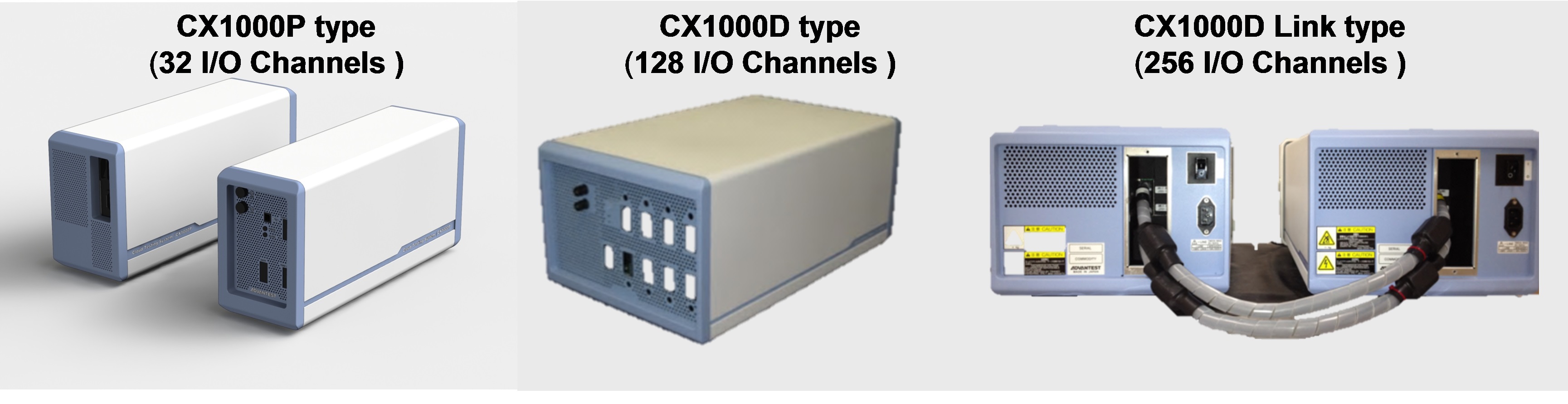
Figure 6: CTS hardware types
The station is provided at zero-rental cost to each CTS subscriber, and only the performance board need be developed, either by the user or an Advantest partner. Standard connectors and cables are provided on demand.
The CX1000P box provides two power supplies, 32 I/O channels, one PMU, one Arbitrary Waveform Generator (AWG) and one digitiser (DGT). Additionally, it contains two reference voltage supplies, one auxiliary power supply and 16 controller signals to control specific use applications.
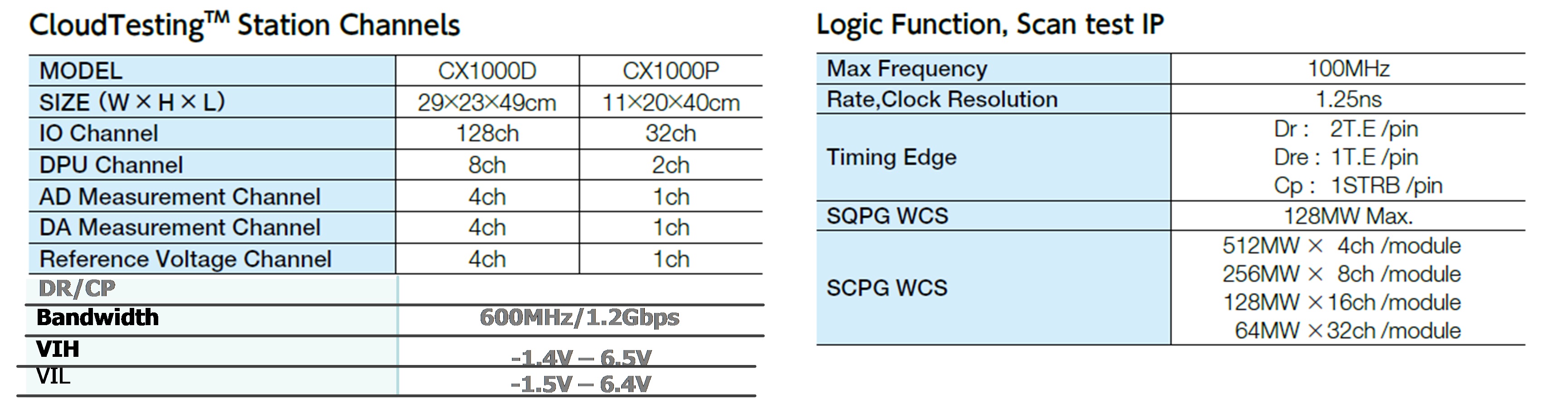
Figure 7: CTS hardware — basic specifications
The CX1000D box provides eight power supplies, 128 I/O channels, four PMUs, four AWGs and four DGTs. As with the CX1000P, the CX1000D provides the same user application control signals. Two CX1000D can be linked offering double the resources, for example 256 I/O channels.
CTS complements a traditional ATE portfolio by providing a flexible, low-cost and efficient test solution for laboratories, R&D, universities and fabless companies working on design and characterisation stages of IC devices. After a successful launch in Japan and the US, Advantest Europe is excited about bringing the service to Europe.
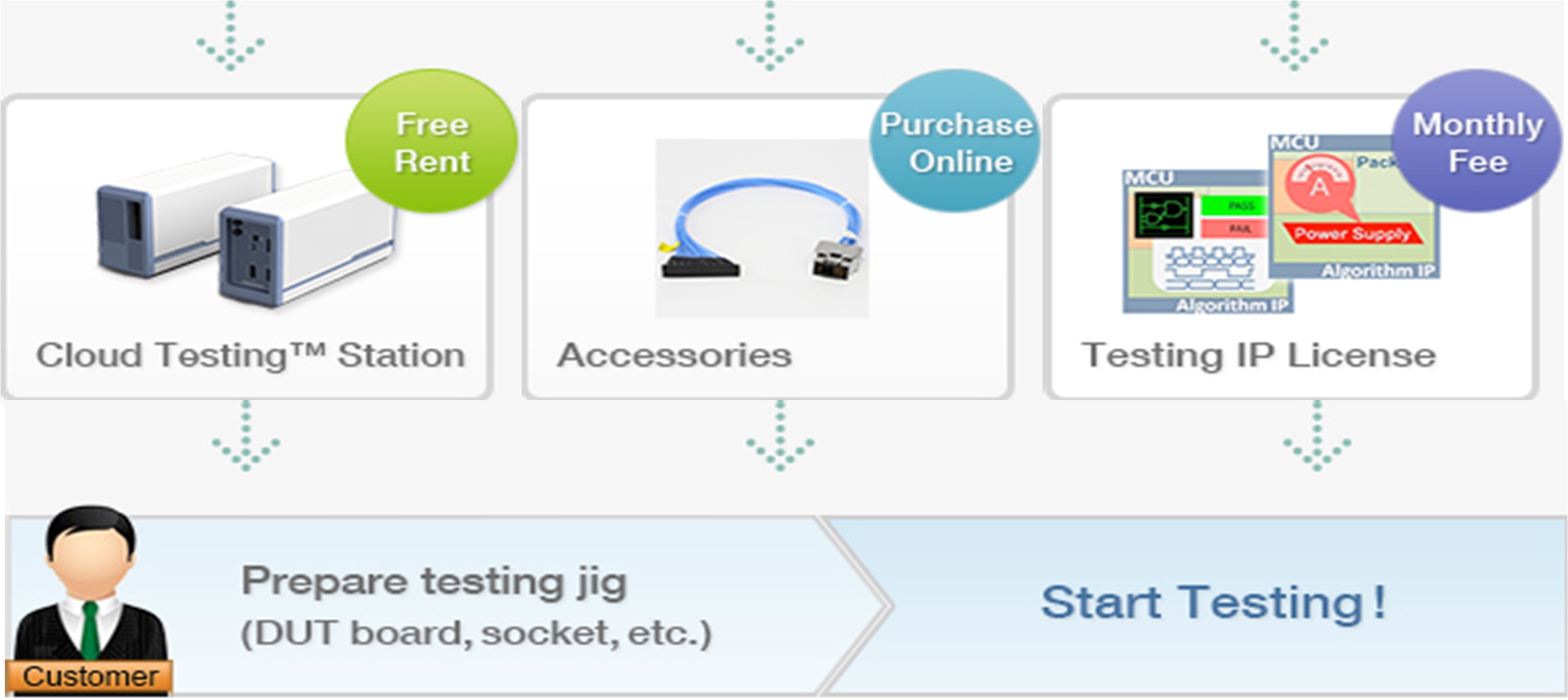
Figure 8: CTS pay-per-use approach
Product Spotlight
APV1111GVY
Panasonic

Panasonic PhotoMOS® Photovoltaic MOSFET High-Power Drivers
| SKU: | |
|---|---|
| Stock: | 3490 |
| Cost: | $3.95 |
