
5 advantages of graphene-based Hall effect sensors
Paragraf’s Dr Hugh Glass outlines the extraordinary technical characteristics of an exciting new electronic device - graphene-based Hall effect sensors.
It is fair to say that graphene has been slow to realise its potential in the electronic device sector, as scientists and engineers have grappled with the challenge of how to manufacture and process the material at scale.
However, many of those obstacles have now been overcome, thanks to the development of a patented technology from Paragraf that allows the manufacturing of large-area, high-quality graphene, currently up to 8” diameter. This highly innovative approach uses a modified deposition method that removes the need for the transfer processes commonly applied in most large area graphene synthesis methods. As a result, graphene can be grown in a uniform, single layer directly on a wide range of semiconductor-compatible substrates, including silicon, silicon carbide, sapphire and gallium nitride, while also being free from metallic contamination.
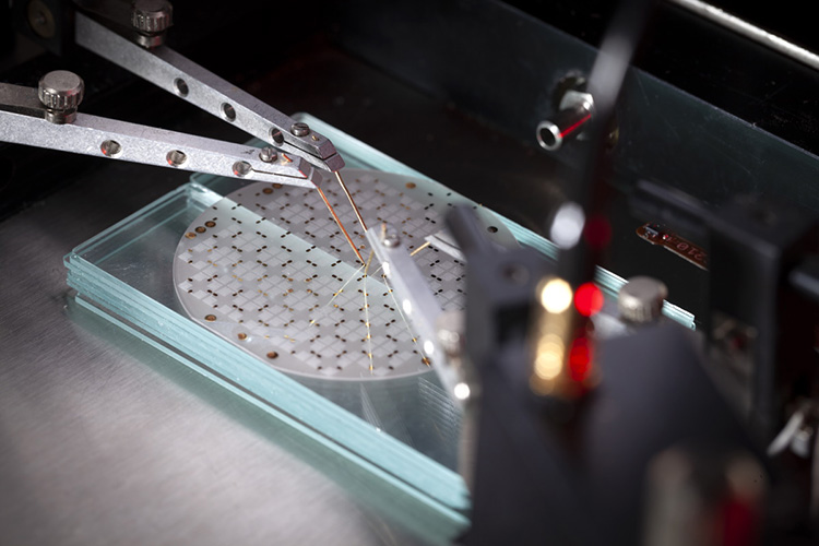
Above: Electrical measurements of a Hall Effect sensor on a wafer
This scalable approach means graphene is now finding some exciting new uses in the electronics sector, for example, through the development of a commercially viable graphene Hall effect sensor. This device can be used for a wide range of applications in many industries including aerospace, automotive and healthcare. They are also ideal for scientific research, including highly accurate magnetic measurements for high energy physics.
Here, we take a look at five crucial advantages of graphene-based Hall-effect sensors.
- More accurate and with better resolution than silicon Hall effect devices: One of the issues with traditional silicon Hall effect sensors is the thickness of the sensing material, which causes the sensing layer to be three-dimensional. This causes field components that are not perpendicular to the sensing direction also to be sensed, and as a result, false signals are produced. This is known as the planar Hall-effect.
Graphene-based Hall-effect sensors lack a planar Hall effect, due to the inherent thinness and truly 2-dimensional nature of monolayer graphene, meaning false signals are not induced. This enables only the actual perpendicular magnetic field value to be obtained, allowing for higher precision mapping of magnetic fields. Also, due to the extremely low noise and high sensitivity of the sensors, a resolution in the sub-100nT region is possible, which is far beyond that achievable with a regular Hall sensor (usually in the 10s-100sµT). - Wider range of temperatures: Another significant benefit that sets graphene-based Hall effect sensors apart from other devices is their wide temperature range. The sensors can be used in extreme cryogenic temperatures at conditions of less than -271°C (1.8K) and currently up to +80°C (353K), with future high temperature variants under development. Crucially, this enables the sensor to be used in superconducting environments, while actually becoming more sensitive.
- Low power operations: Graphene Hall effect sensors also have an incredibly low power dissipation – of the order of picowatts (pW) with nanoamperes (nA) drive current. This means they will not heat cryogenic environments and will save energy compared to other Hall-effect sensors.
- Rugged performance: The new graphene Hall-effect sensors are robust and can be used in extreme environments. As well as being resistant to thermal shock, no electrostatic discharge (ESD) protection is required for the sensors, which can be plugged straight into the mains (220V) without any adverse effects occurring. This makes the sensors easier to handle in industrial and commercial environments.
- Faster and more dynamic: In addition to the benefits mentioned in points 1-4, graphene Hall effect sensors harness the extremely high mobility of the charge carriers in the graphene for faster sensing and a wide operational bandwidth. The sensor also has a highly linear voltage response (less than 0.5% non-linearity over +/- 1T and correctable to 0.01% with a simple third order polynomial correction) and can measure over a large dynamic measurement range (>9T). All of this performance is achieved with the bare sensor, hence with further development and the aid of signal processing electronics, additional performance gains are expected.
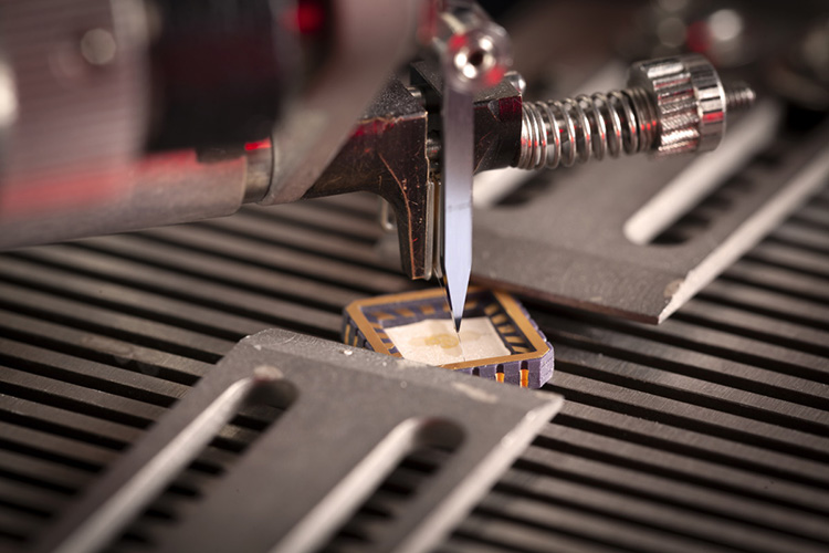
Below: Wire bonding of a Hall Effect sensor to a chip carrier using a wedge bonder
These five advantages show that the new graphene-based Hall effect sensor has enormous potential in the electronics device sector. In terms of development progress, field testing at the Magnetic Measurement Laboratory of the European Organization for Nuclear Research (CERN) has proved that the sensor has negligible planar Hall effect. Therefore, as a 1D magnetic sensor, the signal being measured is a ‘true’ signal only coming from one direction - without interference from signals coming from other directions. The National Physical Laboratory, meanwhile, is investigating the suitability of the sensors in harsh environments.
To conclude, while graphene might have been slow to make an impact in the electronics sector, its time has now clearly arrived.
Product Spotlight
APV1111GVY
Panasonic

Panasonic PhotoMOS® Photovoltaic MOSFET High-Power Drivers
| SKU: | |
|---|---|
| Stock: | 3490 |
| Cost: | $3.95 |
