
The fundamentals of switched mode power supplies
Switched mode power supplies are ubiquitous but often poorly understood. To optimise their use in systems requires an understanding of how the various types and how they operate
Switched mode power supplies (SMPS) are used for desktop PCs (the AC/DC power supply), laptops (the adapter) and the mains charger for a mobile phone. DC/DC converters using the same principles are also embedded in most electronics. The advantage of an SMPS is efficiency. A regulated DC rail simply dropping excess voltage across a series resistor or transistor is around 60% efficient for a linear AC/DC, yet a switching model can be better than 95% over a wide range of conditions. Boosting a DC voltage, changing its polarity or DC/DC conversion with isolation is not possible without the switched mode technique - unless resorting to a motor generator set. The high efficiency results in lower losses and smaller size, weight and cost.
A switched mode power supply operates by ‘chopping’ the input DC or rectified AC at high frequency, at varying duty cycle, with a semiconductor switch which is either fully on or off. The resulting square wave AC is rectified and passed through a low pass filter to average the waveform back to DC. By varying the switching duty cycle, the final DC level can be adjusted and a transformer can be interposed to provide isolation and voltage scaling. Output voltage can now easily be scaled up or down, with or without isolation, at high efficiency. The DC output can also be continuously modulated by varying duty cycle and filtered to generate low frequency sinusoidal AC, the principle of an inverter used in a UPS or variable frequency motor drive.
Converter topologies
There are two basic SMPS topologies, buck or boost for non-isolated converters and their equivalents, forward and flyback in isolated types. The common buck converter is shown in Figure 1. In the circuit, TR1 switches on and off with varying duty cycle, usually at fixed frequency. When on, current passes to the output through inductor L, which simultaneously and linearly builds up a magnetic field with increasing current. D1 is reverse biased and capacitor C1 is charged. When TR1 is off, the energy in the field continues to drive current to the output through D1 which is now forward biased by the reversal of the voltage across the inductor when it swaps from energy storage to energy release. At this time, C1 discharges and varying the duty cycle of switching varies the average output voltage.
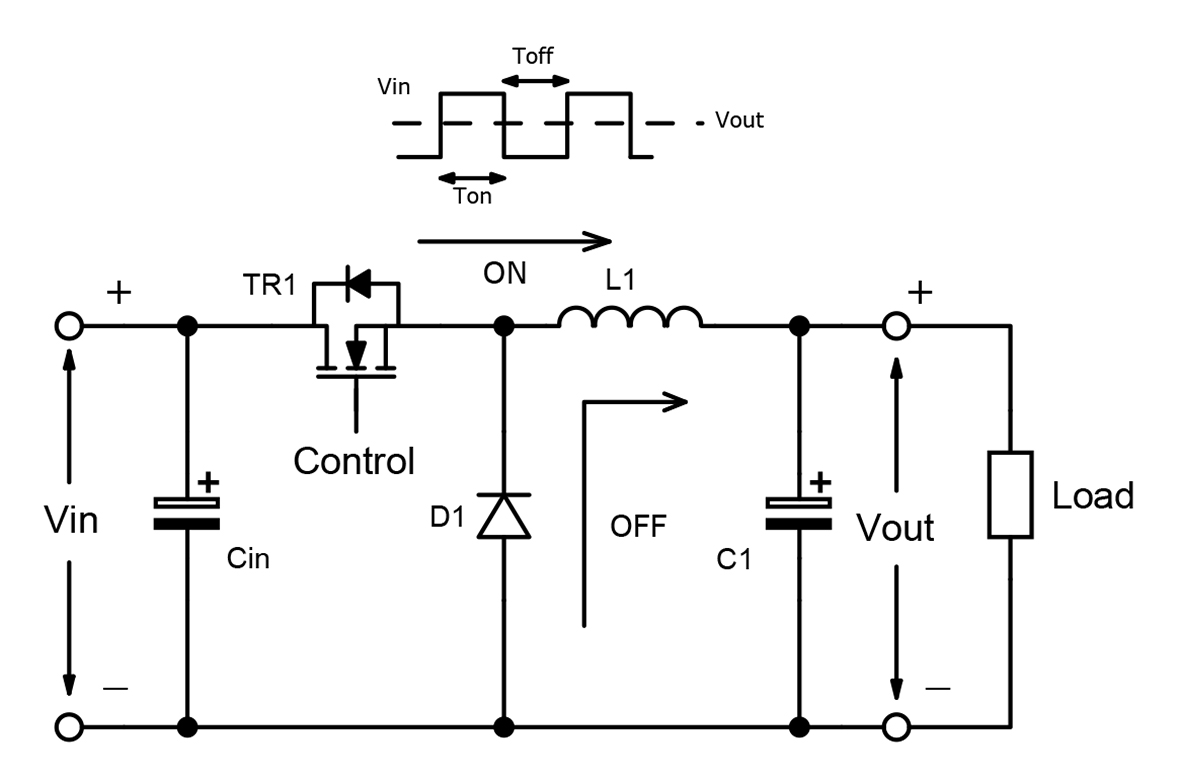 Figure 1: The outline of a buck step-down switching converter outline.
The buck converter only reduces voltage. To increase voltage a boost topology is used (Figure 2). Here, energy is stored in L1 during TR1 on-period and released during the off period, when the inductor voltage flies positive, forward biasing D1 and passing energy to the load. Unlike in the buck converter, with TR1 off, there is no continuing current to the load, so output capacitor C1 has to provide all the load current during this period and is consequently typically much higher value than in the buck converter and passes much higher ripple current.
There are topologies than can both increase or decrease voltage, e.g. a buck-boost converter and a single ended primary inductor converter (SPEIC). These are used where a battery voltage is normally regulated down to a lower value. A SEPIC, for example, allows the battery to discharge from above to below the output voltage, while maintaining regulation and maximum run-time.
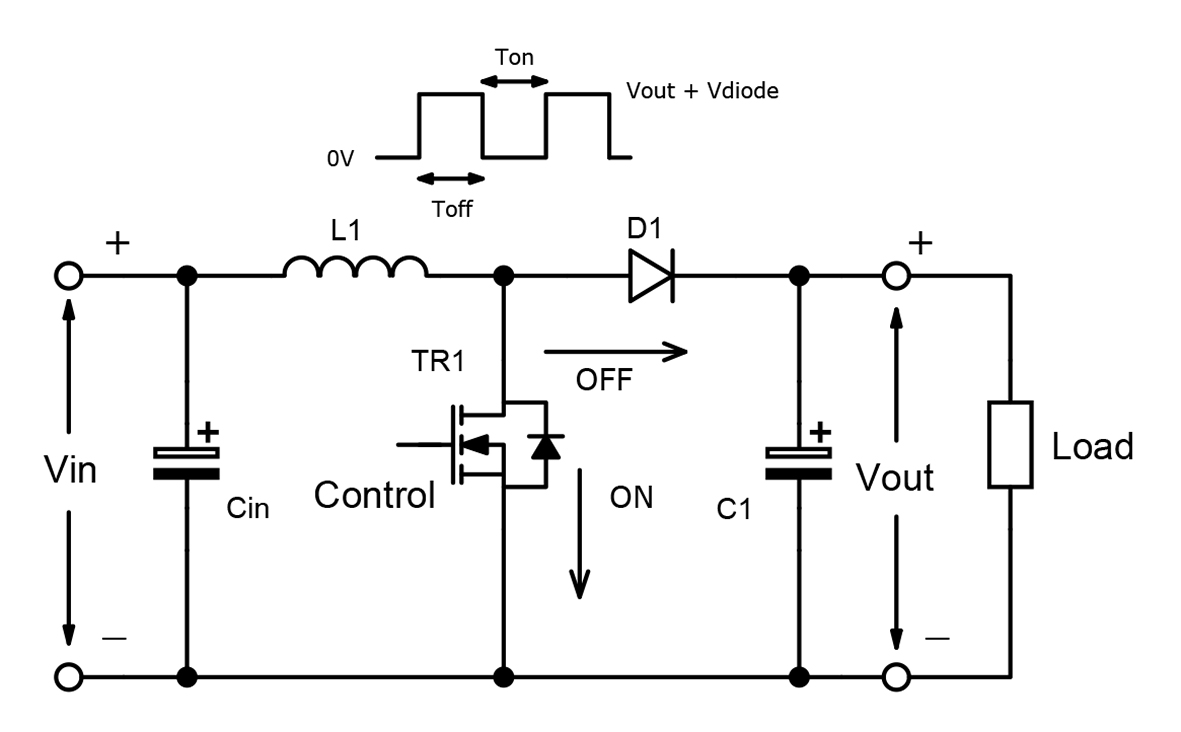 Figure 2: The outline of a boost switching converter.
None of these converters provide isolation. If this is required, there are high-efficiency switching topologies based on forward and flyback techniques.
Isolated switched mode power
The circuit of Figure 3 is a typical single switch, flyback AC/DC converter used at low power. At higher power, a variant of a forward converter might be used. The practical difference between the two topologies is in the fundamental transformer design and in the circuit detail. The forward converter, for example, has a discrete output storage inductor not present in the flyback, where energy is stored in the transformer.
In Figure 3, the input filter has two functions: it attenuates transients on the supply input which might damage the converter and it reduces conducted electromagnetic interference (EMI) generated by the power supply. Any switched mode converter generates some high frequency electrical noise, either differential i.e. between the input lines or common mode i.e. from both lines to ground. The level is limited by national regulations, so a filter which attenuates both types of noise is usually necessary. Input filters are often combined with transient over-voltage protection and in-rush current limiting components.
After filtering, the input is rectified to produce DC, up to around 370V for 240V AC supplies at their maximum tolerance. A bulk capacitor reduces AC line ripple and provides hold-up during short mains interruptions.
Using a bulk capacitor means that current is taken from the line in bursts, at the peak of the mains cycle. This represents a poor power factor, the ideal is a sinusoidal current in phase with the voltage, giving a power factor of unity and low harmonic distortion. Regulations dictate that power factor correction (PFC) should be applied to achieve a value closer to unity for power supplies rated at more than 75W (20W for LED drivers). Although a simple series inductor helps passive PLC, a more efficient option is an active PFC stage, with the bulk capacitor moved to its output. Here, a boost converter takes power over the full mains cycle to produce a higher voltage, with the current actively shaped to be sinusoidal.
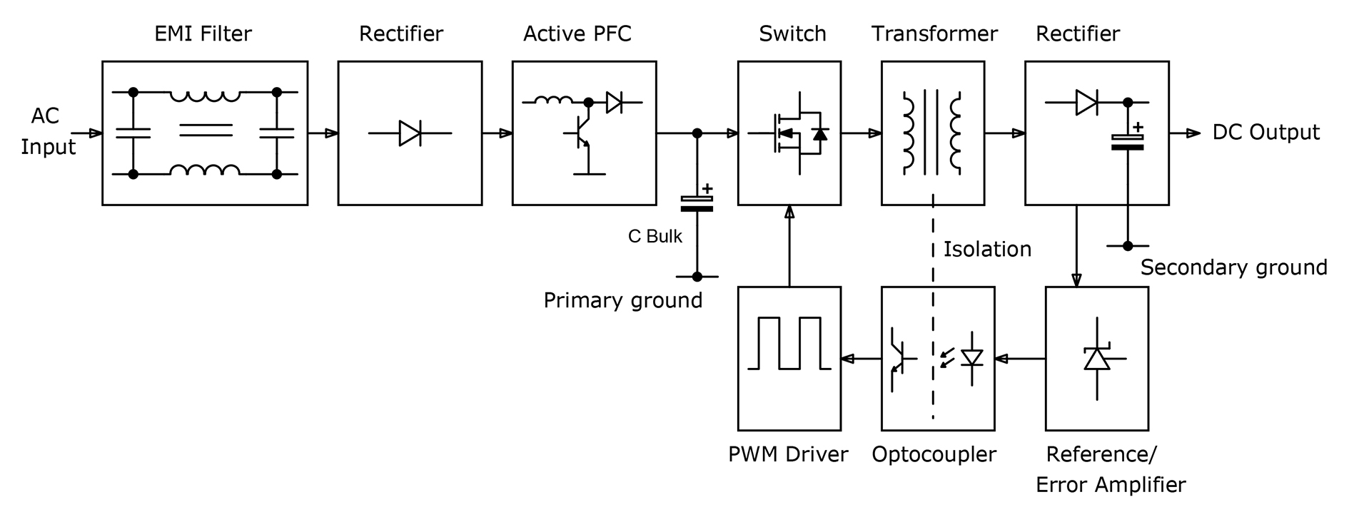 Figure 3: The outline of an AC/DC switched-mode power supply
The boosted voltage is constant for any AC input, so the bulk capacitor can be a smaller value to achieve a given hold-up even at low mains.
The switch block is typically a high voltage MOSFET. The frequency can be fixed, with variable duty cycle to achieve regulation or it can be variable. This can enable quasi-resonant switching for high efficiency, but the changing frequency with load and line variations can make EMI filtering more challenging. In a flyback converter, the switch drives the primary of the isolation and voltage scaling transformer to store energy, which is then passed to the output when the switch is off. While the MOSFET dissipates little while on or off, during switching transitions there can be some overlap of current and voltage, causing significant transient dissipation each cycle. Passive snubber networks are typically used around the MOSFET to control the overlap and reduce losses.
The transformer secondary voltage is rectified and smoothed to generate the desired DC output. The DC value is typically compared with a reference and a correcting signal is passed back to the primary through an opto-coupler to vary duty cycle of the main switch. An increasingly popular technique is to use a separate transformer winding referenced to the input as feedback, which removes the need for the opto-coupler, but the output accuracy is degraded a little.
High power converters
At higher power levels, variants of forward converters are used with multiple switches in bridge arrangements to use magnetics more effectively and share the component stresses. For the highest efficiency levels, resonant converters are increasingly used such as the LLC, or at higher power still, the phase shift full bridge. Efficiencies of around 98% are achieved using these techniques for off-line converters, but at high power, significant heat is still generated and power supplies may feature internal fans or be specified to operate with external forced air. The latest products often give the option of baseplate or even liquid cooling when fan noise is undesirable.
Build versus buy
The performance of off-line power supplies is heavily regulated for safety, efficiency and EMI levels and the cost of approvals almost always favours a bought solution for all but the highest production volumes. Even then, specialist development costs of an in-house design can be prohibitive, and there are also the inventory and production overheads associated with assembling hundreds of discrete components compared to a pre-tested and approved module. Non-isolated parts often do not have the approvals overhead, but modules can still score, with their advanced fabrication techniques typically achieving a smaller footprint than a discrete solution. When communication and control is an application requirement, digital converters and power supplies are the modern techniques to apply.
It is advisable to consult a specialist supplier when selecting an AC/DC or DC/DC converter because, apart from headline specifications, other parameters may affect the application. For example, if output power is only a peak demand, for a motor perhaps, a lower cost converter may be available with a low continuous but high peak rating. The supplier can also assist with selection of a part with the appropriate agency approvals for the target market.
About the author:
Philip Lechner is Technical Specialist, Power, at Avnet Abacus
https://www.avnet.com/wps/portal/abacus/solutions/technologies/power/ac-dc-power-supplies/
.
Product Spotlight
APV1111GVY
Panasonic

Panasonic PhotoMOS® Photovoltaic MOSFET High-Power Drivers
| SKU: | |
|---|---|
| Stock: | 3490 |
| Cost: | $3.95 |
