
SiC and GaN technologies lead the way at PCIM 2016
This year’s PCIM exhibition introduced a whole host of new power products, technologies and applications. Sally Ward-Foxton reports from Nuremberg. This year’s PCIM (power conversion, intelligent motion) exhibition in Nuremberg brought together 436 exhibitors and more than 10,000 visitors from around the world to share the latest in power products, technologies and applications.
As with last year, a lot of attention was given to SiC and GaN products, with GaN finding its way into commercial products and SiC reaching its second (or even third) generations of technology in some places. Meanwhile, silicon MOSFET and IGBT process technologies also continued to improve the performance of these devices, and power modules for all manner of applications showed increased efficiency and more compact form factors. Here’s a round-up of some of the most interesting new things from the show floor.
Million dollar winner
On the GaN Systems booth, visitors had the chance to see the winning entry for Google and the IEEE’s Little Box Challenge, which took the first prize of $1m earlier this year. The competition was to shrink the size of an inverter to 40in3 with 50W/in3 power density or better, with the smallest entry crowned the winner. The winning design from CE+T Power is based on GaN Systems transistors and achieves 145W/in3 and is only 13.77in3 in size. Other GaN Systems customer solutions on display included Egtronics’ 48V, 12kW inverter which is five times smaller than an equivalent design using silicon transistors.
Panasonic Automotive and Industrial Systems showed off several new innovations. These included its X-GaN gate driver, which is for fine control of high frequency switching of the company’s GaN products to ensure maximum performance. It can switch the transistors from 0.5% to 99.5% at 50kHz and includes a precise current source and a negative voltage source.
Another highlight was Panasonic’s thermal interface material made of a thin sheet of graphite. LDPGS (Low Density Pyrolytic Graphite Sheet) is apparently the thinnest thermal solution in the world at just 200µm, and it has a thermal conductivity of 1,950W/mK (five times higher than copper). It’s flexible and can be cut into any shape, replacing the traditional gap filling grease while saving space and weight.

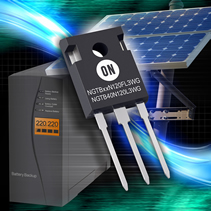
Above: a new power conversion platform from Analog Devices suits renewables, energy storage and HEV infrastructure.
Infineon presented a new power module for hybrid/electric vehicles (HEV) main inverters and generators that is more compact than previous generations of technology would allow. With the engine compartment of these vehicles typically quite cramped, the new HybridPACK DSC module helps save space as it’s only 42 by 42.4 by 4.77mm. HybridPACK DSC’s power range is 40 to 50kW, but more power can be produced by paralleling modules.
The size of these modules is often governed by the power chips, which need space around them for thermal management purposes. In the new HybridPACK DSC module, Infineon has used a technique called double sided cooling (DSC), in which each of the power chips are packed in a metal can to help get heat away faster. Combined with electrically isolating the heat sinks, the thermal resistance has been reduced to 0.1kW (compared to 0.12kW for previous generations).
Analog Devices launched a power conversion platform designed to meet increasing safety regulations in renewable energy systems, energy storage and HEV infrastructure. The regulations for protection from electric shock are strict, which means current measurement needs to be isolated from the power handling circuits and transient signals. Redundant isolated components are usually used, but with the new ADSP-CM41x mixed signal processor at the heart of the platform, they are no longer needed. The ADSP-CM41x has two cores, providing a level of redundancy within the same chip (it has a Certificate of Safety Attestation, VDE-AR-N4105, from TUV-SUD). The platform also uses Analog Devices’ iCoupler digitally isolated gate drivers and a new, compact A-D converter.
The latest in MOSFETs from Toshiba (top) is the fifth generation of its DTMOS process technology, which promises lower EMI noise and an on-resistance (RDS(ON)) reduced by 17% compared to the fourth generation. It’s still based on deep trench etching followed by P-type growth, which narrows the cell pitch and lowers the on-resistance. Thermal coefficient of the on-resistance is also improved. The first DTMOS V parts are 600 and 650V rated and features on-resistance of 0.29 to 0.56Ω.
SiC success
Toshiba also exhibited a second generation of its SiC Schottky barrier diodes. While the properties of SiC reduce heat dissipation and save space, Toshiba’s second generation process technology has reduced the die thickness to allow 1.5x the current density compared to its first generation products. “Significantly higher” non-repetitive forward surge currents (IFSMs) are another effect of the process, according to Toshiba.
Another company showing SiC diodes was Rohm. The company is onto its third generation of SiC Schottky barrier diodes, which boast the lowest forward voltage and reverse current on the market, according to Rohm. The diodes come in 650V rated 6, 8 or 10A versions in a TO220AC package. The company also showed a 1,200V, 180A SiC-based power module which uses its SiC MOSFET and Schottky barrier diode parts. It has a half bridge topology and achieves 77% lower switching loss than traditional IGBT modules. Low switching loss enables higher frequency operation, reduced thermal requirements and smaller peripheral components.
Cree’s SiC specialist division, Wolfspeed, featured two different 20kW DC-DC converter designs powered by its SiC 900V MOSFETs. The first was a full bridge LLC resonant converter with an efficiency of 98.5% and a resonant frequency of 200kHz. The second was a phase shifted full bridge resonant converter, also switching at 200kHz, with an input at 700V and 97.4% efficiency at 50% load. Both designs demonstrated the advantage of SiC MOSFETs over 650V silicon equivalents as the number of transistors used was reduced from 16 to 8 for both of the SiC designs.
Performance IGBTs
Over at ON Semiconductor, IGBTs were the focus of the company’s activities. They have introduced three new 1,200V devices which offer total switching loss (Ets) performance. Two have a VCEsat of 1.7V at rated current and offer 2.7 or 1.7 mJ Ets. The third is optimised for low conduction losses, and offers VCEsat of 1.55V at rated current with Ets of 3mJ. The performance is down to ON Semiconductor’s third generation Ultra Field Stop process technology which uses a wide, highly activated field stop layer below the devices combined with thinner wafers. There’s also a fast recovery diode in the package.
Power Integrations launched a family of IGBT/MOSFET driver ICs with up to 8A output current (without an external booster). The galvanically isolated SCALE-iDriver family uses a communications technology called FluxLink, which replaces older, unreliable optocoupler-based solutions. Instead of an opto-electronic link across the isolation barrier, FluxLink uses magnetic induction to deliver feedback information. The result is an increase in speed and accuracy of communication with less jitter, which increases performance and reliability. And because it’s integrated into the package, rather than being a separate component, it saves space, too.
Allegro previewed its linear current sensor IC (Hall sensor) in a new coreless package, which measures just 6.4 x 6.4 x 1.5mm. It is for sensing up to 150A, and performance is optimised by common mode field rejection of signals from nearby conductors.
Meanwhile, LEM introduced a Hall sensor family of three parts optimised for small currents, from 8 to 100A. Compared to previous versions, global accuracy over the whole temperature range (-40 to 85°C) is 3.5x better, at 0.5% of IPN.
Product Spotlight
APV1111GVY
Panasonic

Panasonic PhotoMOS® Photovoltaic MOSFET High-Power Drivers
| SKU: | |
|---|---|
| Stock: | 3490 |
| Cost: | $3.95 |
