
Seeking a solution for voltage changes and reverse flow operation
Bi-polar power, bi-directional power supplies for automotive and audio systems that are immune to input voltage changes while generating power and enabling reverse flow current are possible, proposes Victor Khasiev
Most electronic systems depend on power voltage rails that are either positive or negative, but a few applications require individual rails that can be both. In these situations, positive or negative power is supplied by the same terminal (i.e. the output voltage of the supply can be adjusted through its entire voltage range, smoothly transitioning across polarity).
Some automotive and audio applications, for example, require - in addition to traditional voltage sources - power supplies that can function as a load and sinking current from the output terminals. Regenerative braking in automotive systems is one example. Single terminal, bipolar power supplies are documented, but solutions that can operate during input voltage drops, such as cold crank conditions, while continuing to provide bidirectional functionality are not.
There is a solution immune to input voltage changes while generating power and enabling reverse current flow, that is, from output to input.
Bi-polar, bi-directional circuits
Figure 1 shows a two-stage power supply, which centres around a four-quadrant controller (stage 2), U1. This converter is fed by an intermediate bus converter, VINTER (stage 1), supplying an output voltage in a range of 12 to 24V, nominally 12 to 16V, matching the nominal voltage range of the standard automotive battery rail. The output of the complete two-stage converter is ±10V delivering a 3.0A current to the load. The output voltage is controlled by the voltage source ‘control’ signal at the ‘CTRL’ pin of controller U1.
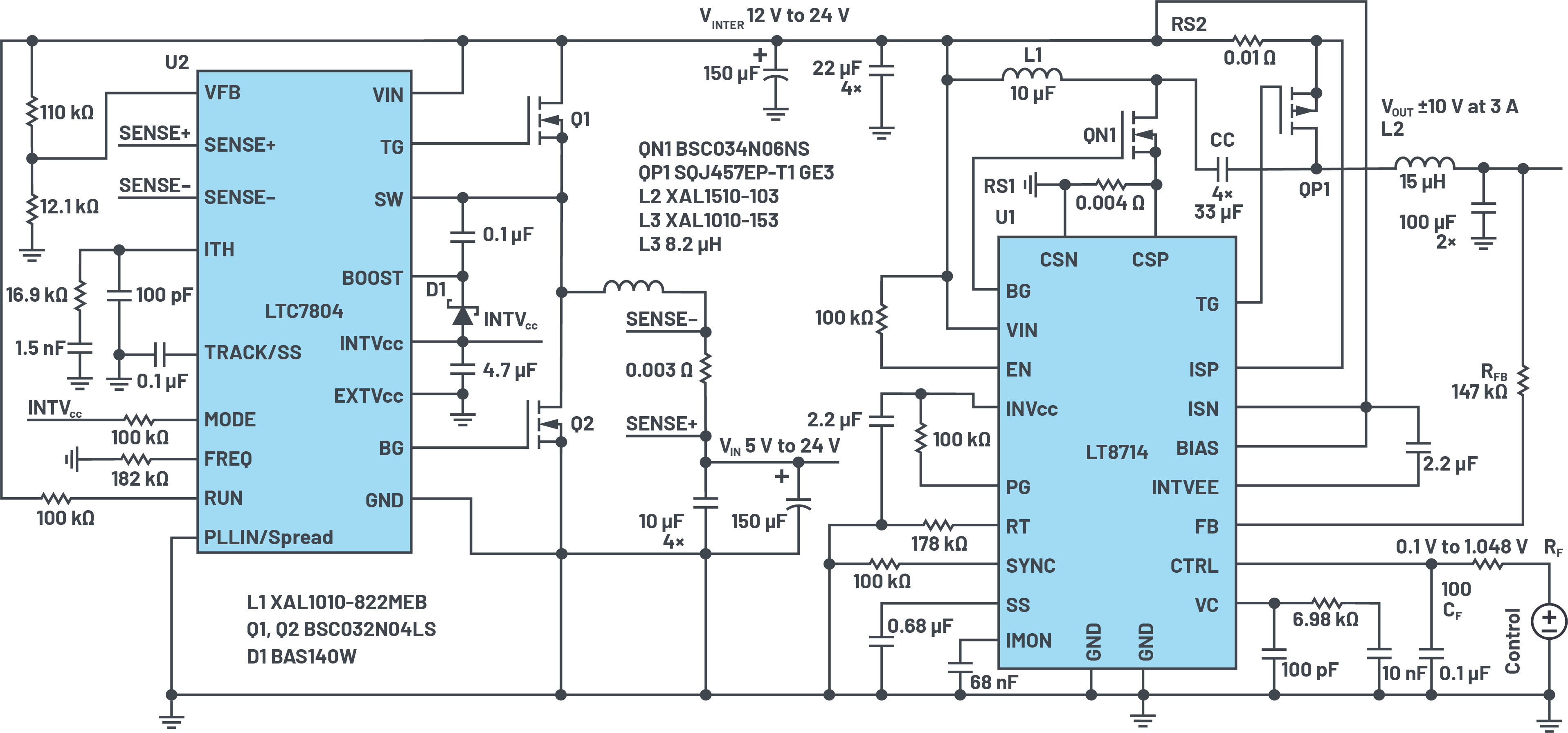 Figure 1: Electrical schematic of bi-polar, bi-directional, two-terminal power supply: VIN = 5 V to 24 V, VOUT = ±10 V at 3 A.
The low-pass filter CF, RF alleviates sharp changes in control voltage. The power train includes two MOSFETs, n-channel QN1 and p-channel QP1, two discrete inductors, L1 and L2 and an output filter. The choice of two discrete inductors instead of a single coupled inductor extends the range of suitable magnetics and allows the use of previously approved and tested chokes.The outputfilter is composed exclusively of ceramic capacitors because of the dual polarity nature of the output.
The input voltage range of the full two-stage converter is 5.0 to 24V, to cover cold cranking voltage drops in automotive electronics and brownouts in industrial applications. The boost converter (stage 1), based on controller U2, maintains the voltage of the intermediate bus at or above 12V whenever the converter is enabled.The powertrain of the boost converter includes inductor L3 and MOSFETs Q1and Q2.The two-stage arrangement allows normal operation of the downstream four-quadrant converter to deliver ±10V to the load at all operational conditions.
Sourcing current
The oscillogram in Figure 2 shows the circuit of Figure 1 in action When an input voltage is applied at VIN, the boost converter regulates its output, VINTER, to 12V if the input falls below this level. If VIN exceeds the 12V typical for a nominal 12V automotive rail, then the boost converter enters Pass-Thrumode or wire mode. In this mode, the top MOSFET Q1 is enhanced at 100% duty cycle, always onoperation,sonoswitchingoccurs. The voltage, VINTER, applied to a four-quadrant converter remains relatively stable at a level equal to VIN.
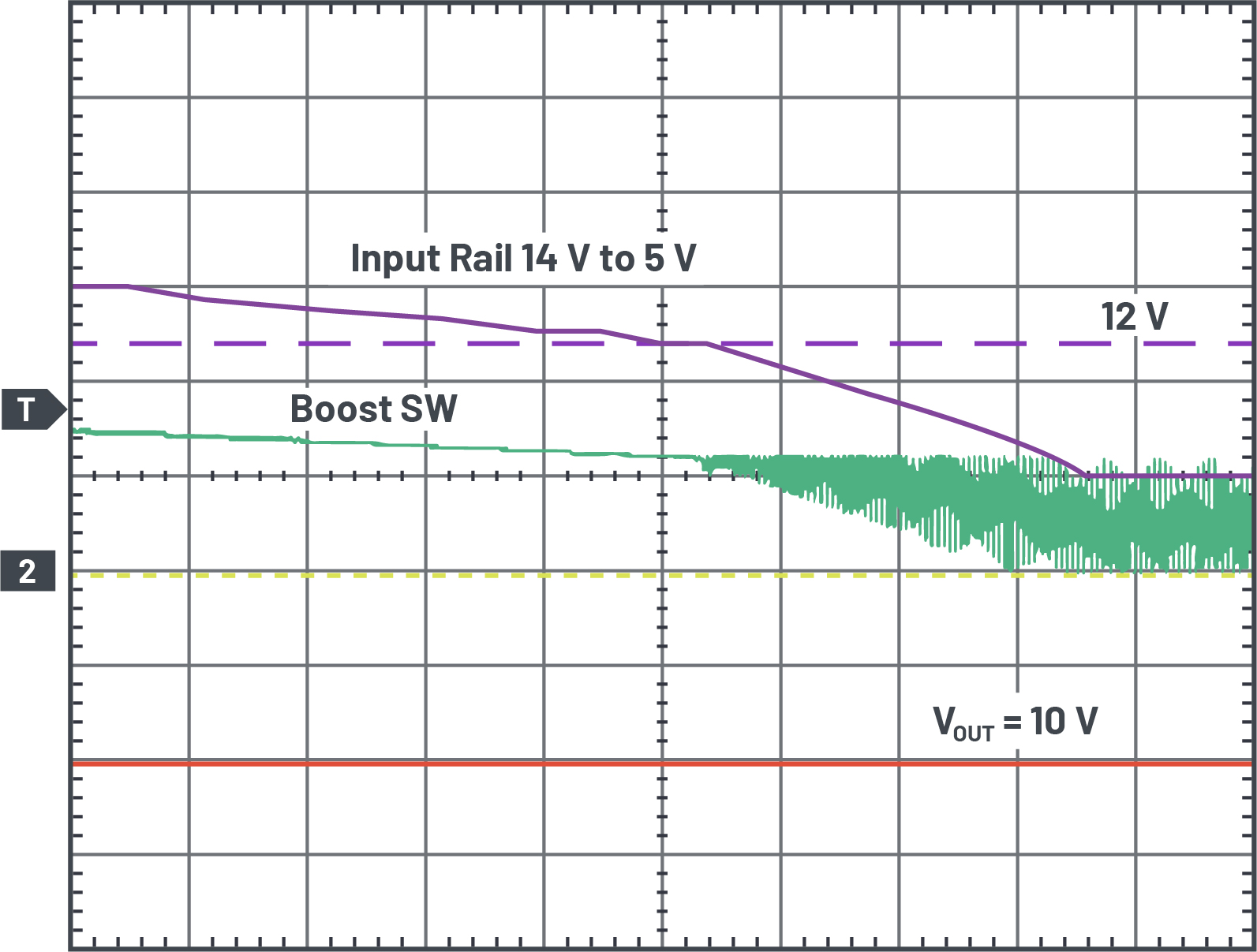
Figure 2: Waveforms showing VIN dropping from 14V to 5V. VIN = 5.0V/div, VOUT = 5.0V/div, boost SW = 10V/div, and the time scale is 200µs/div.
This approach increases system efficiency over a typical two-stage device (namely, a boost converter followed by buck/inverting).This is because efficiency in Pass-Thru mode, where the system will spend most of its time, can be near 100%, essentially turning the power system into a single-stage converter. If the input voltage drops below 12V, for example, during a cold cranking event, then the boost converter resumes switching to regulate VINTER to 12V. This approach allows the four-quadrant converter to deliver ±10V, even when facing sharp drops of the input voltage.
When the control voltage is at its maximum, in this case, 1.048V, the converter output is +10V. If the control voltage is at its minimum (100mV), the converter output is -10V. In this example, the control voltage is a 60Hz sinusoidal signal frequency with a peak-to-peak amplitude of 0.9048V. The resulting converter output is a 60Hz sinewave with a peak-to-peak amplitude of 20V. The output smoothly changes from -10V to +10V.
In this mode of operation, the four-quadrant converter regulates the output voltage. The output voltage is sensed by U1 through the resistor RFB at its FB pin. The voltage at that pin is compared to the control voltage, and from that comparison, the converter’s duty cycle (i.e. the gate signal on QN1) is adjusted to keep the output voltage in regulation. If VINTER, Control or VOUT changes, the duty cycle is modulated to regulate the output accordingly. MOSFET QP1 switches in sync with QN1 for synchronous rectification to further maximise efficiency.
this two-stage regulator can operate as a current source or a current sink. In current sink mode, current and power flow in reverse from the output, VOUT, to the input, VIN. This is important for automotive electronics and some audio systems.
During reverse current flow, the four-quadrant converter regulates output current that passes from VOUT to VIN; the converter does not regulate voltage in this mode. The four-quadrant controller senses output current as the voltage drop across the sense resistor, RS2 in Figure 1, and regulates its duty cycle to keep this voltage drop at a set value, 50mV, for this solution.
As a four-quadrant converter generates voltage on the VINTER bus that exceeds the specified minimum, the boost converter enters Pass-Thru mode with top MOSFET Q1 always on and delivers the preset value of the output current to VIN (load) terminals with the smallest losses possible.
This mode of operation was benchtop verified and tested. To do so, the VOUT of the circuit in Figure 1 was connected to a lab power supply set to 12.5V and the VIN to an electronic load, with the current through the converter set to 4.5A.
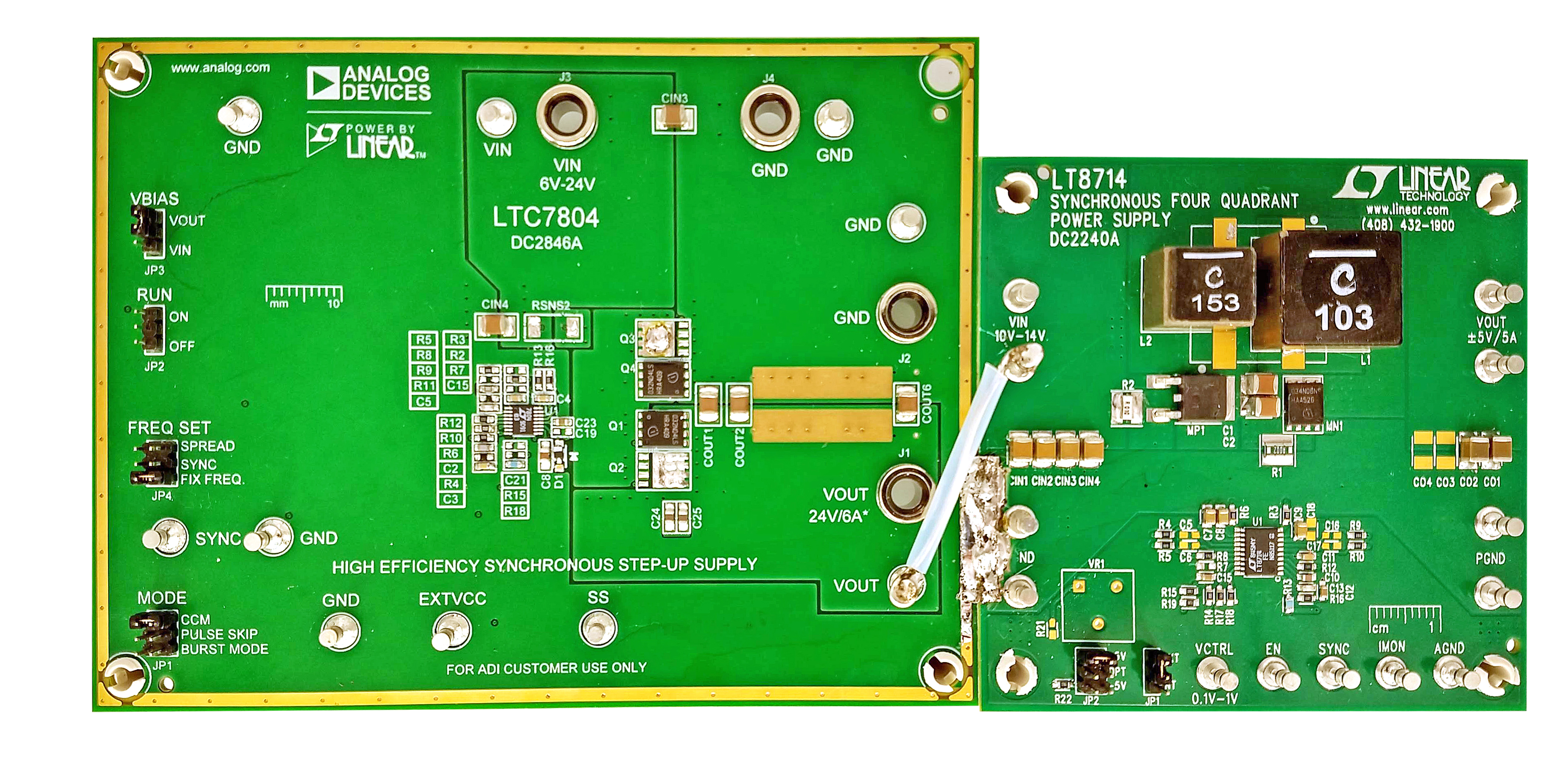 Figure 3: Left, the LTC7804 (DC2846A) and the LT8714 (DC2240A) on the right.
Figure 3 shows a photo of the converter, an off-the-shelf DC2846A boost converter demonstration circuit and a DC2240A four-quadrant converter demo circuit, soldered together.
The two controllers selected for this application were the LT8714 four-quadrant controller, featuring high efficiency synchronous rectification and the LTC7804 synchronous boost converter. The latter has an internal charge pump, providing switching free, Pass-Thru, 100% duty cycle operation.
Conclusion
A few specific features of the converter contribute to the performance of the overall solution: synchronous rectification yields high efficiency, and simple, dedicated control scheme provide an easy interface to any type of host processor and external control circuitry. The solution presented here solves the problem of unstable input voltages, including fast transients, and guarantees stable output voltage in all operating conditions.The combination of devices chosen facilitates the design of bi-polar, bi-directional power supplies and enable near-100% efficiency operation as an intermediate supply in automotive and industrial environments.
Abou the Author
Victor Khasiev is a senior applications engineer at Analog Devices (ADI) with extensive experience in power electronics and holds two patents, including efficient PFC solutions and advanced gate drivers.
Product Spotlight
APV1111GVY
Panasonic

Panasonic PhotoMOS® Photovoltaic MOSFET High-Power Drivers
| SKU: | |
|---|---|
| Stock: | 3490 |
| Cost: | $3.95 |
