
Feature-rich systems demand configurable PMICs
Feature-rich systems demand flexible and configurable, 20V, high current power management ICs (PMICs), argues Steve Knoth, senior product marketing manager, Analog Devices
The advance of technology has increased the feature content of all electronic systems, while reducing available space. Mobile phones have touchscreens, flashlights, power-save modes and sophisticated cameras while automotive dashboards once featured only basic AM radio and a few gauges, but now are packed with elaborate instrumentation, satellite radio, Bluetooth, GPS and other cell phone-based network connections, multi-coloured lighting and a myriad of USB ports. The same applies to industrial rugged computers which contain barcode readers, large screens, hard drives, and illuminated keyboards and medical electronic devices today contain sensors, multi-intensity flashlights, gauges, and power-save modes.
What hasn’t changed is the need for power. As portable and system electronics features increase, so do their power requirements, especially when GPUs, FPGAs, microcontrollers and microprocessors, PLDs, DSPs and ASICS are used.
These complex digital devices require multi-rail, high power density power supplies featuring high current, low voltage, and fast transient response. These stringent demands are combined with specific high performance requirements, such as low noise or digital control, placing significant stress on power supply designers to deliver cutting-edge solutions.
Power system design challenges
Modern electronic system designers are challenged to meet restrictive space requirements, limited operating temperature ranges and noise specifications. Integration levels are high to save PCB space, requiring efficient power components to keep temperatures in check. For example, today’s automobile dashboards are packed with electronic systems that operate in a high ambient temperature environment, so temperature monitoring and reporting is a critical requirement, particularly for power management components. A system controller can respond to over-temperature alerts with mitigation steps to prevent system over-heating, such as turning off less critical functions or throttling back performance of processors, displays, and network communication.
From a power supply perspective, even the most basic dashboard automotive infotainment console requires several low voltage power supply rails (output levels) at several amps of total current and a premium console requires far more. Traditionally, low voltage rails have been produced by a multitude of tiny point of load (PoL) discrete power regulator ICs, or large, highly integrated PMICs. Many PMICs often have more rails than are needed, require a large circuit footprint, and can be under-powered for some rails, defeating the purpose of the additional integration.
Another potential design challenge is feature creep, or the slow change of product specifications as development marches forward, such as changes to input and output voltages and output currents. Feature creep can wreak havoc on the selection of ICs and associated discrete components. In the best-case scenario, when a system specification is changed after the board layout is set, a voltage can be tweaked by swapping out a few resistors on an adjustable output converter. In a worst-case situation, several ICs must be replaced with non-pin-out-compatible ICs when updated current levels exceed the switch current rating of the incumbent converters. This can require IC-, board-, or system-level requalification, increasing costs and adding schedule delays for even the smallest feature change.
The solution is a power IC that offers more outputs than purely discrete, single, or dual output ICs, but takes less space, and costs less than a full-featured PMIC. This in-between regulator is a multi-output power IC that can provide a small footprint with a configurable number of moderately powered rails. Ideally, such an IC could be configured to output a wide variety of voltages and currents to accommodate changes in power requirements that arise during development, avoiding requalification cycles and reducing product time to market. Furthermore, it could operate at input voltages above 5V with high efficiency to allow use in a variety of application spaces, such as from 12 to 18V wall adapters. Integrated safety and monitoring features, wide temperature range operation, and innovative package design with high thermal performance are also desirable.
Versatile PMIC
The LTC3376 is a highly integrated, general-purpose power management device for systems which require multiple low voltage power supply rails. It can be configured to provide one to four independent regulated outputs from an input of up to 20V, with 15 possible output current configurations and a total output current of up to 12A (Figure 1). This flexibility makes it suitable for use in a variety of multi-channel applications, including telecomms, industrial, automotive, and communications systems.
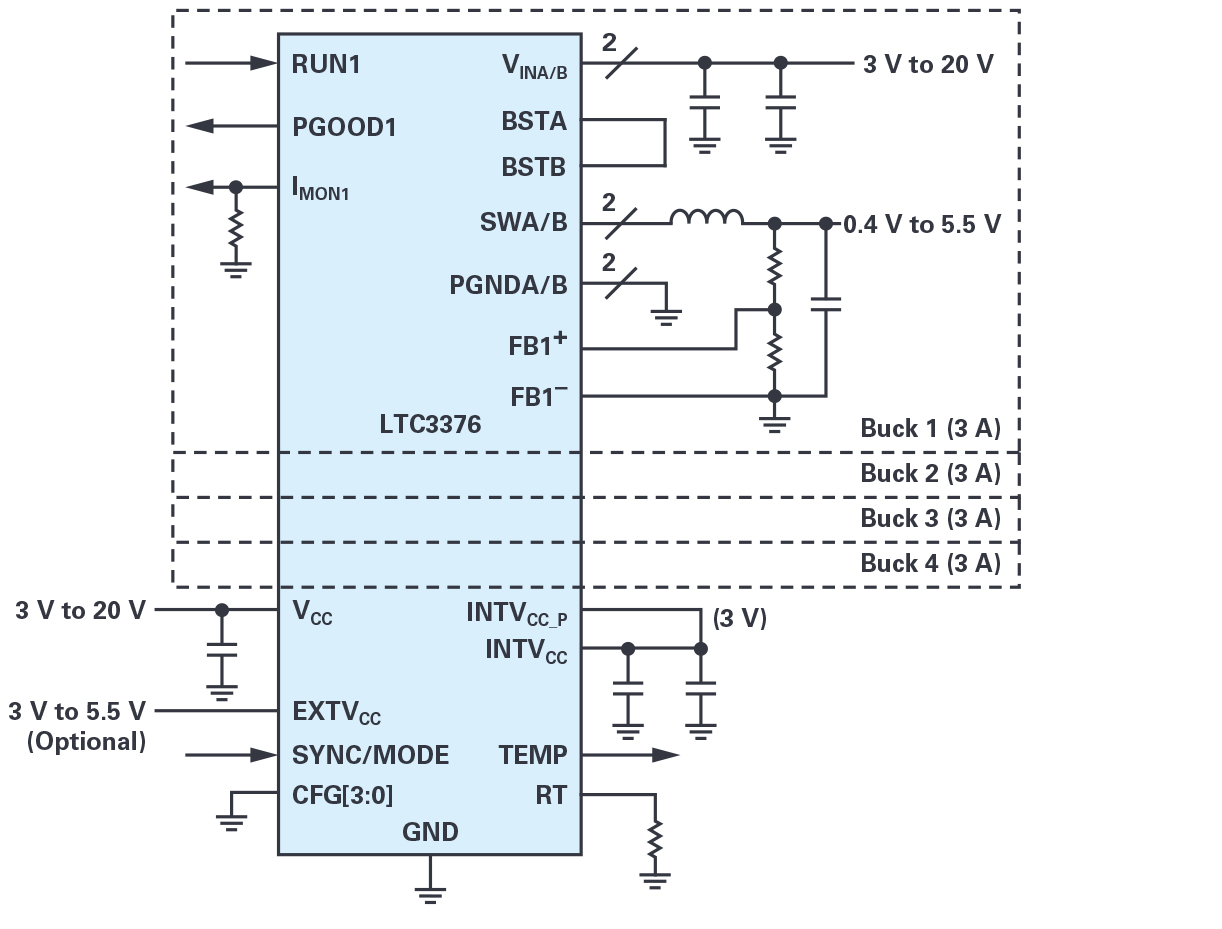
Figure 1: Simplified block diagram for the LTC3376
There are four independent buck regulator channels and eight configurable 1.5A power stages with flexible sequencing and fault monitoring, delivering a total available output current of 12A. Peak buck efficiency is 96% with ±1% output voltage accuracy on all channels. Each channel can be powered from an independent 3.0 to 20V input supply and has an output voltage range down to 0.4V. Adjacent outputs can be combined in parallel with a single shared inductor to simplify the circuit. The DC/DC converters are assigned to one of 15 power configurations via pin-strappable CFG0 to CFG3 pins. External barium strontium titanate (BST) capacitors are not required since they are integrated into the package.
The PMIC’s switching regulators operate in Burst Mode (power-up default mode) for higher efficiency at light loads and forced continuous PWM mode for lower noise at light loads. The switching regulators are internally compensated and need only external feedback resistors to set the output voltage. The buck converters have input current limiting, soft start to limit inrush current during startup, differential output sense, and short-circuit protection. The device has a programmable and synchronisable 1.0 to 3.0MHz oscillator with a 2.0MHz default switching frequency.
The quiescent current with all four converters enabled is only 42µA. There are also four power-good pins indicating when an enabled DC/DC converter is within a specified percentage of its target output and current monitors for external monitoring of each buck’s load. There is also an EXTVCC pin for improved efficiency, precision ‘run’ pin thresholds for power-up sequencing, a die temperature monitor output (readable via an analogue voltage on the temperature pin) for internal die temperature and an over-temperature function that disables the bucks at high die temperatures in case of an overload condition.
The LTC3376 is available in a compact, 64-ball, 7.0 x 7.0mm flip chip BGA package. E- and I-grades are specified over an operating junction temperature range of –40 to +125°C.
Configuration choices
The device can be set up into 15 different output configurations. These are a single inductor, single output 12A buck where all the power stages are internally ganged together to produce maximum current output; four possible dual-buck combinations with two inductors total with the total output current summating to 12A; five triple-buck combinations totalling 12A each with three total inductors and five quad-buck configurations of up to 12A each with four total inductors (see Figure 2).
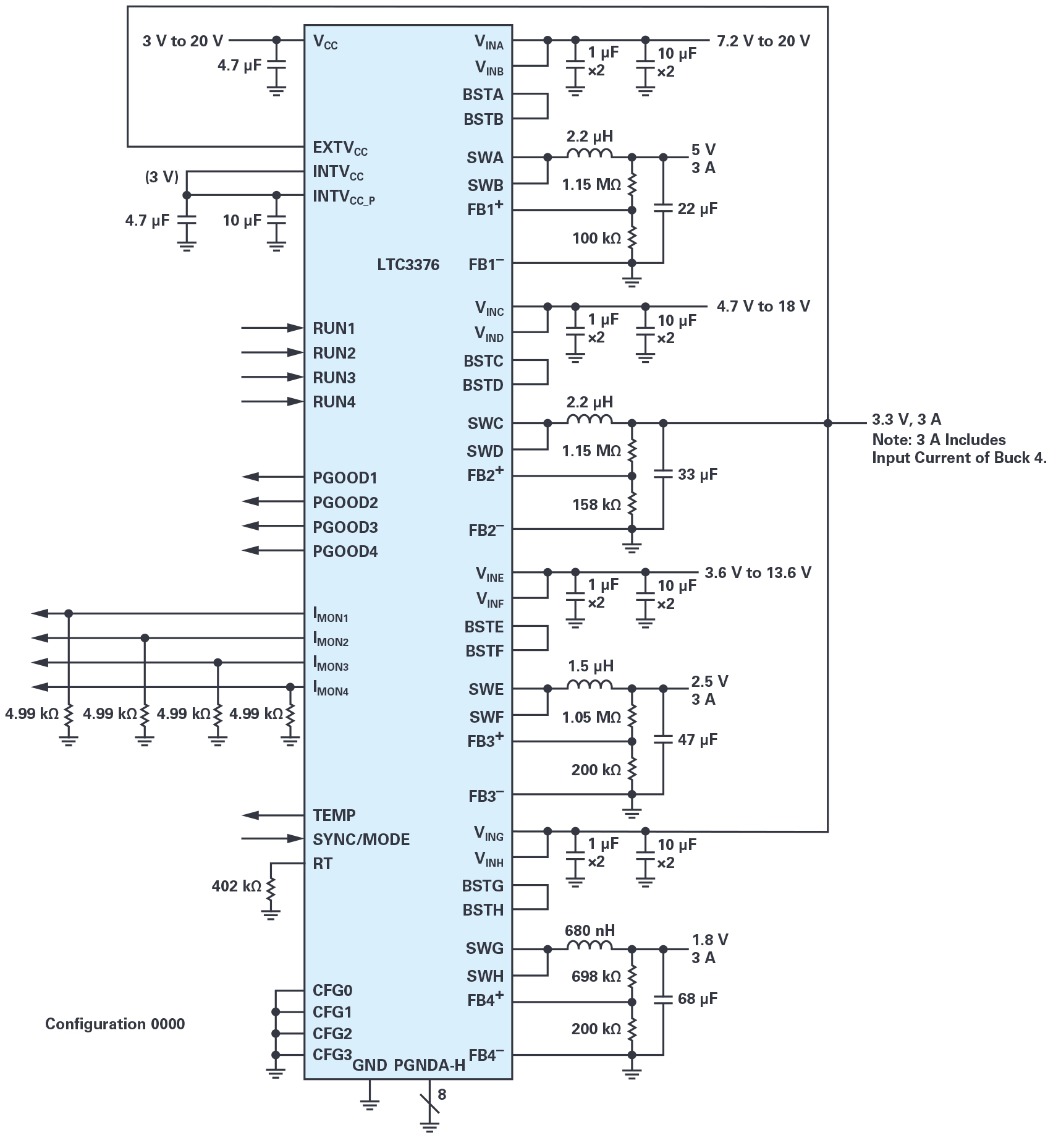 Figure 2: Typical quad-output application circuit
This level of flexibility for output configurations makes adjustment easier when requirements change in the design process. There is no need to qualify a new IC when the LTC3376 can remain in place.
Space constraints
Packaging techniques contribute to the compact, thermally efficient solution afforded by the device. Within the BGA, the internal construction uses copper pillars in lieu of bond wires. Internal boost capacitors and an integrated substrate ground plane improve EMI, which is less sensitive to PCB layout, says the company (Figure 3). Within the die, the power devices are arranged to evenly spread power dissipation.
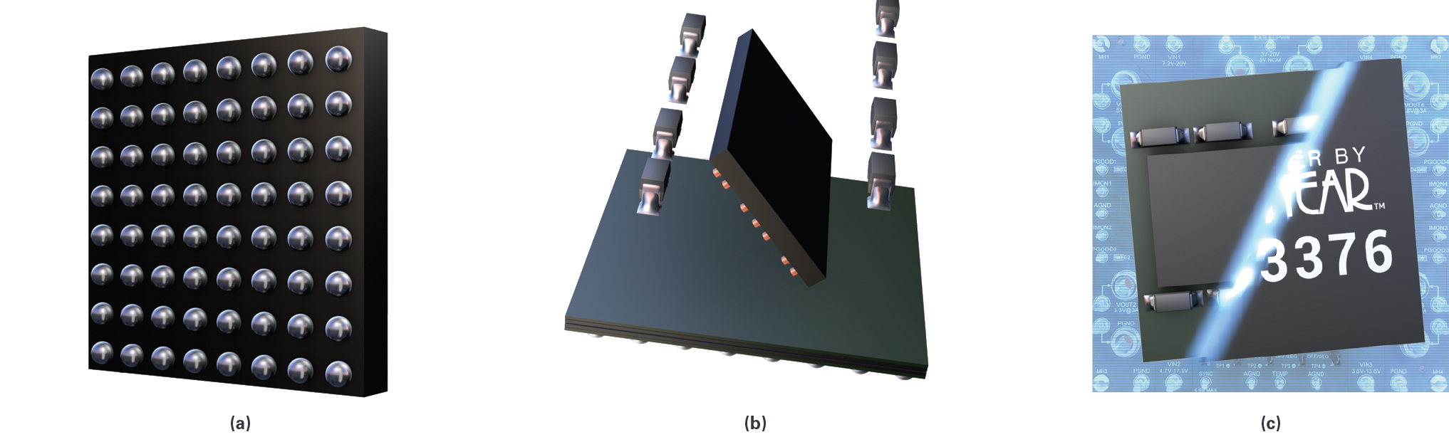 Figure 3: LTC3376 flip chip package with (a) ball grid array, (b) copper pillars under die, and (c) integrated bypass capacitors
Figure 4 shows the LTC3376 in a quad, 4 x 3A buck, with an active area of just 15 x 29mm.
Safety and protection
Safety features monitor and protect the systems it powers. Power failure conditions are reported by each buck’s associated PGOOD pin. Each buck regulator features a current monitor that produces a current at the IMON pin that is proportional to the average buck load current.
To prevent thermal damage to the LTC3376 and its surrounding components, the LTC3376 incorporates an over-temperature function. When the die temperature reaches 165°C (typical), all enabled buck switching regulators are shut down and remain in a shutdown state until the die temperature falls to 155°C (typical).
Replacing multiple discrete power regulator ICs or bulky PMICs in today’s feature-rich devices and equipment with a single, quad, or octal multi-output power IC is a wise choice. The LTC3376 pin-configurable PMIC is an example of this new generation of multi-output power ICs. The digitally programmable PMIC allows system designers to mitigate the impact of inevitable power block system changes and feature creep, while reducing product time to market, development and upgrade costs.
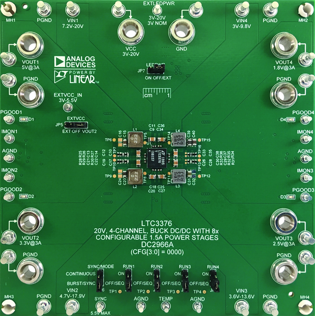
Figure 4: The LTC3376 demonstration board for a 4 x 3A buck with 5.0, 3.3,Analog Devices
Product Spotlight
APV1111GVY
Panasonic

Panasonic PhotoMOS® Photovoltaic MOSFET High-Power Drivers
| SKU: | |
|---|---|
| Stock: | 3490 |
| Cost: | $3.95 |
