
Computing in cars
Designing reliable hardware is challenging the automotive industry, says Jan Preibisch, application marketing manager, Nexperia
Autonomous driving requires tremendous computational resources. The current trend of high-level advanced driving assistance system (ADAS) architectures is a central design; uncompressed video, light detection and ranging (lidar) and other sensor data is sent directly to central computing units.
Depending on the resolution and sensor types, high-speed interfaces are used to send the data from the sensor devices, such as cameras, to the central processing unit (often called ADAS box or ADAS processing unit). As the number of cameras and sensors, like zonal lidar, is increasing, it is clear that the requirement of fast data processing is also increasing.
Ordinary PC-like computing platforms are not powerful enough for the data processing demands of automotives. Some ADAS reference implementations resemble mid-range server-like architectures, with dedicated GPUs optimised for self-learning algorithms. Within the computing unit multiple high power microchips need to operate and communicate, consuming vast amounts of energy.
Reliability and functional safety are important for ADAS applications whereas in self-driving cars, redundant systems are typically used for safety functions like electronics braking or steering.
Architectures for ADAS
The design community has discussed distributed versus centralised ADAS; low-level ADAS implementations are often distributed and high-level ADAS concepts are rather centralised. The reason for this is that algorithms can make better and more reasonable decisions when using the data of multiple sensors at the same time. The pre-processing of the data near the sensor potentially increases the latency and reduces the ability to identify and observe and predict and object’s behaviour based on various sensor data simultaneously.
Hence, the architecture of high-level ADAS concepts is a star-shaped topology, with one or more high speed computing units in the centre and sensor units placed around the car.
This choice has two consequences. Firstly, there are many high-speed communication links between sensors and the central unit to transmit raw data with low latency, and secondly, the computing power of the central unit has to be significant to process the data from various sensors simultaneously and make reasonable decisions (see Figure 1).
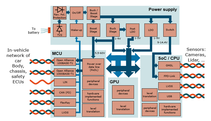
Figure 1: System overview of centralised ADAS computing unit
There is no fundamental difference between the principal architecture of a PC, a mid-range server and a high-level ADAS processing unit. There is a power supply, CPUs and GPUs, microcontrollers for interfacing and microcontrollers to monitor various parameters, loading firmware, turning on and off several parts of the system.
These parts may be significantly different in PCs, servers, and ADAS applications. However, in none of these applications can microcontrollers function alone, they need peripheral devices, resistors, inductors, capacitors, quartz and discrete semiconductors in the form of bipolar transistors (BJTs), MOSFETs, standard logic like gates and buffers, ESD protection, Zener, p-n and Schottky diodes are required.
Although an increasing amount of functionality has been integrated, discretes play an important role in system design because of four main factors, namely flexibility, reliability, power and cost.
The variety of discretes available allows designers to tune the application by selecting the right discrete, rather than redesigning the IC. Reliability comes from the fact that a discrete component only fulfills one functionality, so the production process and testing can be optimised.
Reliable single-function devices can be manufactured much more efficiently than a complex device. For high current applications like power supplies, the ability to use a discrete to separate the power part from the IC is important.
To handle high currents, devices that act as switches or regulators must be large in order to keep the current density inside the device under a certain limiting value. From a system perspective, it is better to have a large switch or regulator as a dedicated discrete device optimised for this application and to keep the controlling IC separate.
Separation allows using a smaller and cheaper IC because they are not heated up by the current that is being controlled. This consideration does not only lead to increased system performance but also to lower system costs, as a large IC is usually more expensive than a discrete component.
As the same discrete components are used in various applications, the high volumes lead to much lower prices than ICs.
Discrete components come in various shapes. Twenty years ago, engineers used through hole packages, where the leads of the package penetrate the PCB. These are still favoured for DIY projects and prototyping due to ease of handling. For mass production, however, the surface mount device (SMD), where the device is soldered on the surface of a PCB, is popular.
Package types
The most famous discrete SMD package is the SOT23, introduced by Phillips Semiconductors 50 years. It allows much denser packing of devices on a PCB and on both sides.
The original SOT23 is a three-pin package often used for BJTs, small signal MOSFETs and (dual) diodes. There is also the SOT457 (or TSOP6, SOT23-6), the six-pin version, used for dual BJTs and small-signal MOSFETs or logic devices, and the SOD323 which is the two-pin diode version.
The package’s plastic is always the same size and the leads are bent down to be soldered onto the PCB. The PCB area needed to solder a three- or six-pin package is roughly 4.6 x 4.5mm. Central ADAS computing units and more sophisticated body control units increase the demand for a smaller alternative that provides the same reliability.
Figure 2 shows a motherboard of a standard PC with 62 discrete devices in SOT23 packages; a comparable amount of discretes is required for an ADAS.
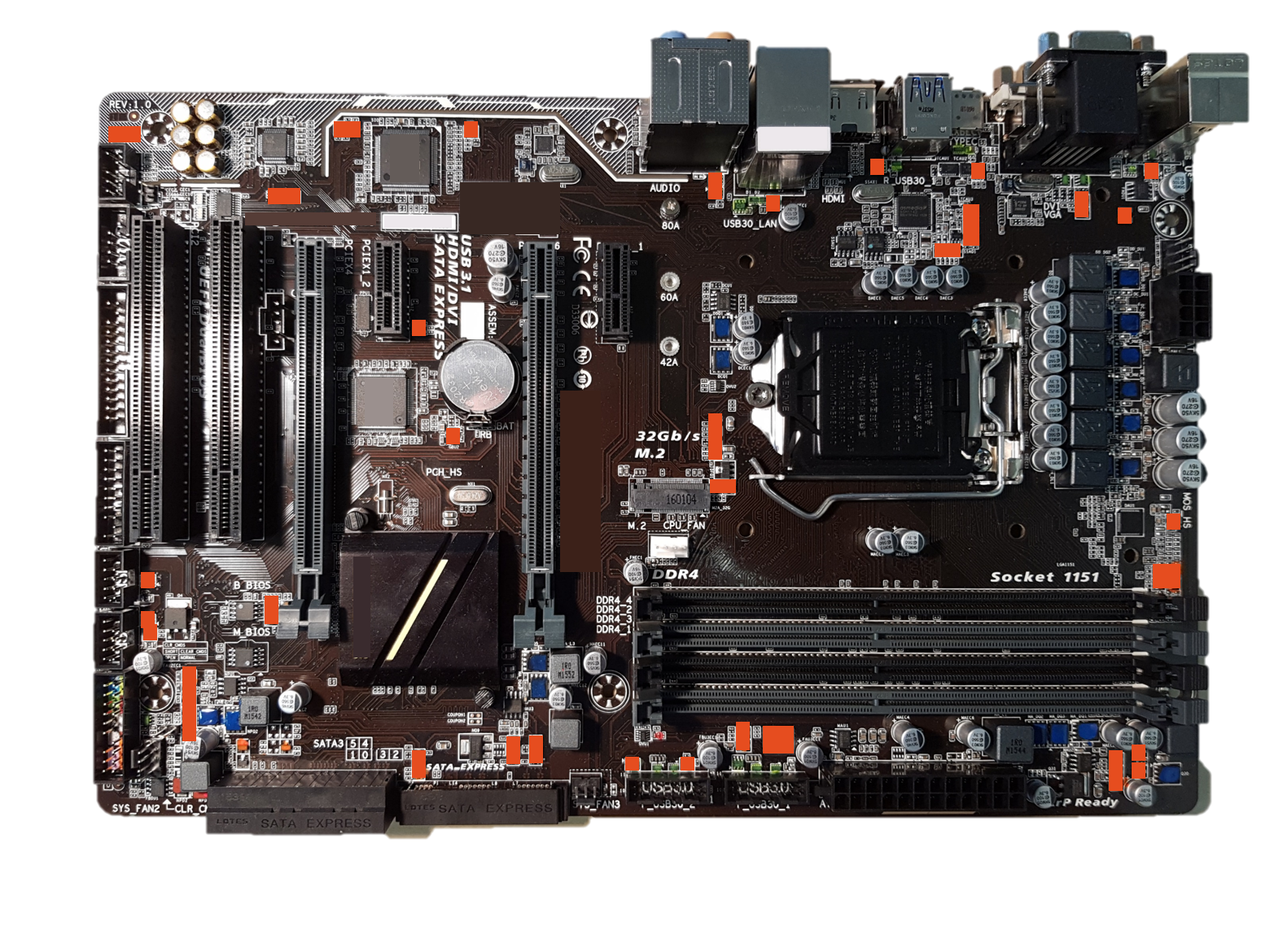 Figure 2: This standard PC motherboard contains 62 discrete semiconductors in SOT23 packages
Modern ADAS computing platforms claim to use one to two CPUs and four to eight GPUs, for a total of around 50 to 250 discrete devices in an ADAS computing unit. Clearly, a miniaturised alternative of the SOT23 is required for space-efficient system designs.
This alternative is the discrete flat no-lead, DFN, package. In Figure 3, the DFN package has approximately the same space inside the package as an SOT23, while being much smaller in total. The footprint required on the PCB to solder the DFN package is 80% smaller than required for the SOT23. It can house the same silicon as a SOT23 can, so the electrical parameters do not change, only the outline of the footprint gets smaller, due to the removal of the leads.
To attach to the PCB, the plastic underneath the metal that belongs to the lead inside the DFN package is removed. This way, it can be directly soldered to the PCB without requiring leads outside the plastic.
The electrical parameters of the SOT23 and DFN are nearly identical. Additionally, the DFN package offers less parasitic capacitance and inductance, from the removal of the leads.
Inspection
It is necessary to assure during production that a solder joint is both electrically and mechanically sound. This is usually done by x-ray diagnostics or camera inspection (also called automated optical inspection or AOI). X-ray inspects ball grid arrays (BGAs) and other hidden solder connections. AOI inspects leaded packages by optically evaluating the meniscus the solder paste forms at the side of the leads. AOI is preferred as, compared to x-ray, it is significantly cheaper and faster.
The solder joint is usually hidden underneath a DFN package. A side-wettable flank is a tin-plated metal strip at the side of the package which means an optically inspectable meniscus is formed at the side of the DFN package, allowing to use the cost-efficient AOI tooling already in place for SOT23.
The mechanical reliability of the solder joint between a DFN package and the PCB fulfills all automotive norms and is tested accordingly.
When leadless packages were introduced for high-power MOSFETs in automotive motor control applications, some designers raised concerns about the reliability of the solder connections, as the package expands when the device heats up and shear forces apply to the solder joints leading to micro cracks.
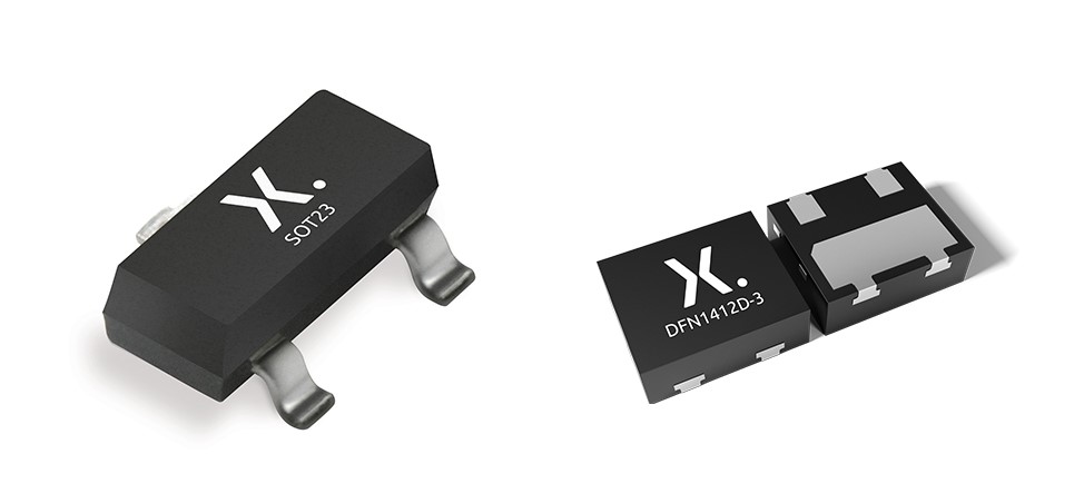 Figure 3: Standard SOT23 package (left) and leadless DFN1412D-3 (right)
Designers of automotive power applications choose the cupper clip-bonded LFPAK (Loss-Free PAcKage), which combines the benefits of a DFN package and external leads that can mitigate the mechanical stress.
For peripheral discretes used in the surrounding CPUs, GPUs and microcontrollers and usually housed in SOT23 packages, the same MOSFETs have to handle high currents and will inevitably heat up whereas most devices in SOT23 run at low power and self-heating is usually not a system- critical effect.
While powerful MOSFETs usually have package sizes of 5.0 x 6.0 or 8.0 x 8.0mm or even larger, DFN alternatives 1.4 x 1.2mm or even smaller. The force applied on the solder joint during elevated temperatures is therefore significantly smaller (Figure 4). This enables DFN packages to be considered a reliable alternative for SOT23 in critical applications like ADAS processing units.
Thermal performance
A second benefit when using DFN packages is that due to the internal structure, the thermal performance is much better.
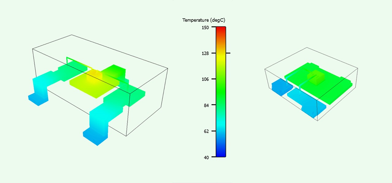
Figure 4: Thermal simulation of SOT23 (left) and DFN1412D-3 (right). (Drawing not to scale)
Figure 4 shows a thermal simulation of a SOT23 and a DFN1412D-3, with the same silicon inside both. The simulations considers a dissipated power inside the silicon of 250mW. In the SOT23 package, the heat that is generated inside the silicon has to dissipate through the leads to PCB. The PCB and, to a very small degree the leads, radiate the heat to the surrounding environment, which is assumed to have an ambient temperature of 25°C. In the DFN package however, the heat is dissipated through the metal heatsink inside the package directly to the PCB. The thermal connection of the DFN package is significantly better than that for the SOT23 package.
In this simulation, it leads to a difference in temperature of the silicon of 25°C. This difference is significant and has two main implications. Firstly, it allows higher power operation in a package and, the device runs cooler in the ordinary operation. This is directly related to an extended lifetime of the device in the application, leading to an increased overall reliability.
The discussion around ADAS is very often focused on software implementations, the latest algorithms and sensors. To bring a system to market however requires a highly reliable, automotive grade hardware platform. Other considerations for the ADAS design engineer are system-critical CPUs and GPUs and the surrounding discrete silicon devices.
Novel automotive grade DFN package provide an alternative to classic leaded package allowing to safe significant amount of space on the PCB enabling a high level of integration. By having even better thermal performance and highest reliability, these packages provide a basis to bring high-level ADAS computing units into mass market production.
High-level ADAS computing units have a high demand of peripheral discrete components that allow for highest reliability and small packaging size to enable high integration. The industry standard SOT23 is available and widely used but its technology is large and occupies significant board space. DFN technology allows developers to house the same electrical functionality in significantly reduced package size allowing the use of an 80% smaller footprint.
Additionally, to the space savings, the technology leads to reduced operating temperature resulting in an increased system reliability.
DFN alternatives exist for the whole SOT23 family.
Product Spotlight
APV1111GVY
Panasonic

Panasonic PhotoMOS® Photovoltaic MOSFET High-Power Drivers
| SKU: | |
|---|---|
| Stock: | 3490 |
| Cost: | $3.95 |
