
Architecture shrinks power supplies
The proliferation of intelligent electronics, automation, and sensors in industry and automotive environments has increased performance criteria for power supplies. Zhongming Ye, senior applications engineer at Analog Devices, explains how a regulator architecture simplifies EMI design, size, efficiency, and thermal proficiency.
Power supply requirements can be reduced for ceramic capacitors by using a high efficiency, high frequency, low EMI DC/DC converter. The price of the multilayer ceramic capacitors (MLCCs) has risen sharply over recent years, tracking the expansion in the number of power supplies used in automotive, industry, data centre and telecommunications industries.
Ceramic capacitors are used in power supplies on the output to lower output ripple, and to control output voltage over-shot and under-shot due to high slew rate load transients. The input side requires ceramic capacitors for decoupling and to filter EMI due to their low ESR and low ESL in high frequency.
The quest to increase the performance of industrial and automotive systems calls for increases in data processing speed of several orders of magnitude, with an increasing number of power-hungry devices squeezed into microprocessors, CPUs, SoCs, ASICs, and FPGAs. Each of these complex device types requires a number of regulated voltage rails, typically, 0.8V for cores, 1.2V and 1.1V for DDR3 and LPDDR4, respectively and 5.0V, 3.3V and 1.8V for peripheral and auxiliary components. Buck (step-down) converters are widely used to produce the regulated power supplies from a battery or a DC bus.
Ceramic applications
The proliferation of advanced driver assistance systems (ADAS) in automotive design has dramatically increased ceramic capacitor usage rates. With the rise of 5G technology in telecommunications, where high performance power supplies are required, ceramic capacitor usages will also significantly increase. Core supply currents have increased from several Amps to tens of Amps, with very tight control of supply ripple, load transient over-shot/under-shot, and EMI features that require additional capacitance.
In many cases, traditional power supply approaches cannot keep up: overall solution size is too big, efficiency is too low, circuit design is too complicated and the bill of materials (BoM) is too expensive. For example, to meet the tight voltage regulation specifications for a fast load transient, a large number of ceramic capacitors are required at the output to store and source significant currents arising from load transients. The total cost of the output ceramic capacitors can reach several times that of the power IC.
Higher power supply operating (switching) frequencies can reduce the effect of transients on output voltage and reduce the capacitance requirements and overall solution size, yet higher switching frequencies usually result in increased switching losses, reducing overall efficiency. Is it possible to avoid this trade-off and meet transient requirements at the very high current levels demanded by advanced microprocessors, CPUs, SoCs, ASICs, and FPGAs?
The monolithic Silent Switcher 2 buck regulator family addresses the challenges of size, current capability, efficiency and EMI performance. The LTC7151S monolithic buck regulator uses Silent Switcher 2 architecture to simplify EMI filter design. Valley current mode reduces the output capacitance requirement.
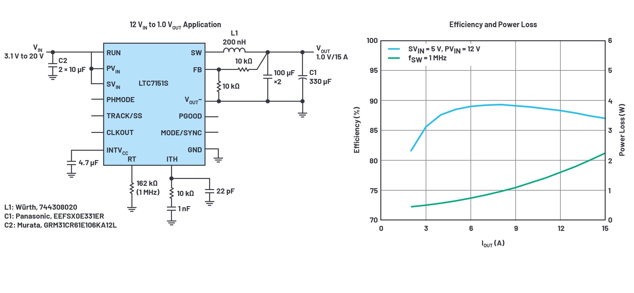
Figure 1: Schematic and efficiency of a 1MHz, 15A buck regulator for SoCs and CPUs
Figure 1 shows a 1MHz, 1.0V, 15A solution for SoC and CPU power applications where the input is typically 12 or 5.0V and can vary from 3.1 to 20V. Only input and output capacitors, an inductor and several small resistors and capacitors are necessary to complete a power supply. This circuit can be modified to produce other output voltages down to 0.6V. The negative return (to the V pin) of the output rail enables remote feedback sensing of the output voltage close to the load, minimising feedback errors caused by voltage drops across board traces.
In this example, an LTC7151S Silent Switcher 2 regulator is used. It has high performance integrated MOSFETs in a 28-lead, thermally enhanced 4.0 x 5.0 x 0.74mm LQFN package. Control is via valley current mode. Protection functions are built-in to minimise the number of external protection components.
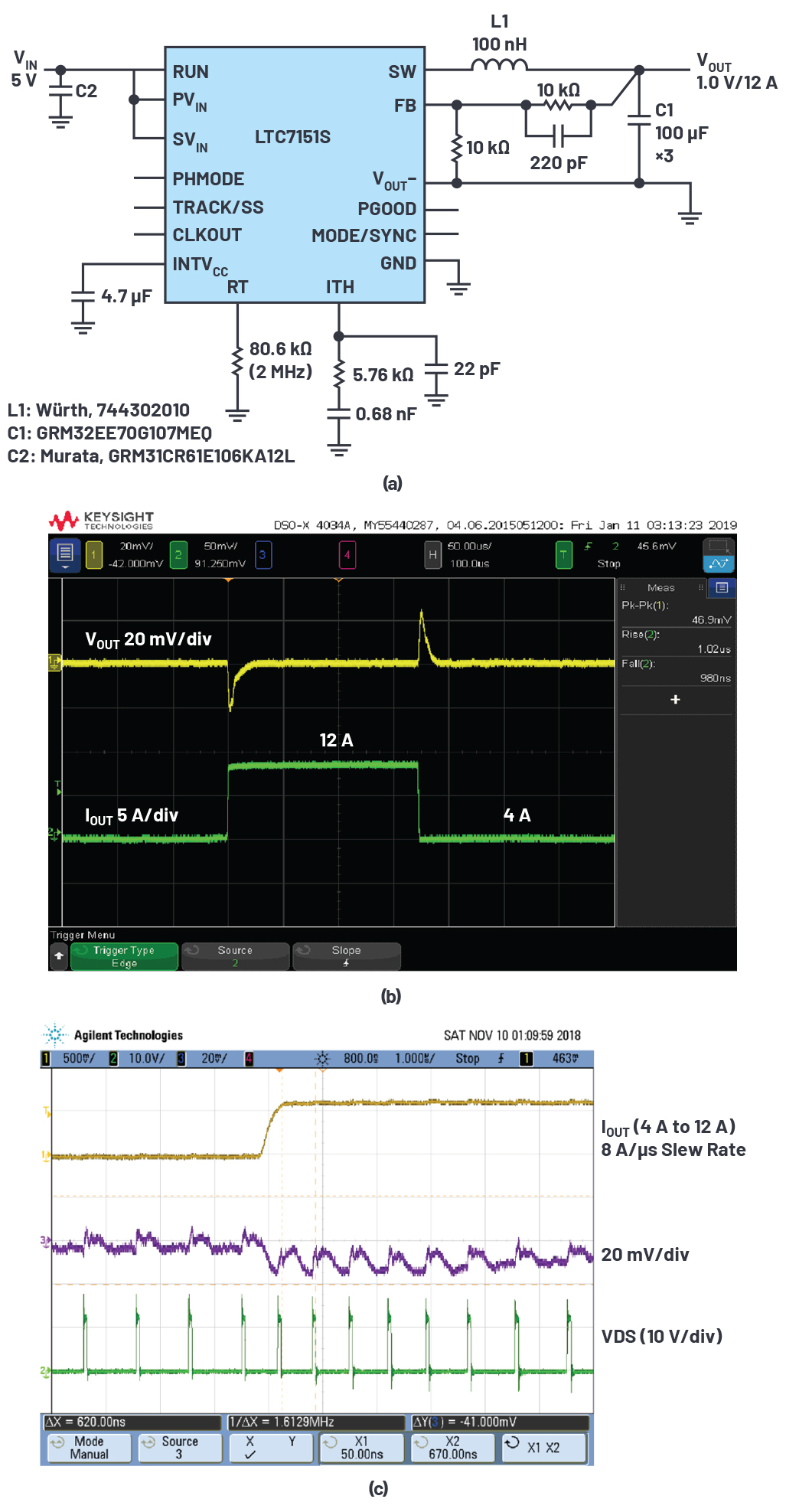
Figure 2: The LTC7151S’s 5.0V input to 1.0V output runs at 2MHz
The minimum on-time of the top switch is only 20ns (typical), enabling direct step-down to core voltages at a very high frequency. Thermal management features enable reliable and continuous delivery current up to 15A from input voltage up to 20V without heat sink or airflow. This makes it suitable for SOCs, FPGAs, DSPs, GPUs and microprocessors in telecomms, industry, transportation and automotive applications.
The wide input range enables its use as a first-stage intermediate converter, supporting up to 15A at 5.0 or 3.3V to multiple downstream point-of-load or LDO regulators.
Controlled transients
Typically, an output capacitor is scaled to meet requirements for loop stability and load transient response. These specifications are particularly tight for power supplies that serve processor core voltages, where load transient over-shoot and under-shoot must be well controlled. For example, during a load step, the output capacitor must step in, instantaneously supplying current to support the load, until the feedback loop brings up the switch current enough to take over. Typically, over-shoot and under-shoot are suppressed by installing a significant number of multi-layer ceramic capacitors at the output side, fulfilling charge storage requirements during fast load transients.
Additionally, or alternatively, pushing the switching frequency higher can improve fast loop response, but at the price of increased switching losses.
There is a third option. Regulators with valley current-mode control can dynamically change the regulator’s switch Ton and Toff times to almost instantaneously meet the demands of load transients. This allows for significantly reduced output capacitance to meet fast response times. Figure 2 shows the results of the LTC7151S responding to a load step from 4.0 to 12A with 8A/µs slew rate. The controlled on-time (COT) valley current-mode architecture allows the switch node pulses to compress during the 4.0 to 12A load step transition. About 1µs after the start of the rising edge, the output voltage starts its recovery, with over-shoot and under-shoot limited to 46mV peak-to-peak. The three 100µF ceramic capacitors (Figure 2a) are sufficient to meet typical transient specifications (Figure 2b). Figure 2c shows typical switch waveforms during a load step.
Confined spaces
MOSFETs, drivers, and hot-loop capacitors are integrated in the 4.0 x 5.0 x 0.74mm package. Keeping these components close reduces parasitic effects, allowing for fast turn on/off of the switches with very narrow deadtime. The conduction loss of the anti-parallel diode of the switches is greatly reduced. The integrated hot-loop decoupling capacitor and built-in compensation circuit also eliminate design complexity.
The 20ns (typical) minimum on the top switch allows for very low duty ratio conversion at high frequency, enabling the designer to take advantage of very high frequency operation (such as 3MHz) to reduce the size and value of the inductor, input capacitor, and output capacitor. This is practical for limited space applications, such as portable devices or instruments in automotive and medical applications. Bulky thermal mitigation components such as fans and heat sinks are not necessary when using the LTC7151S, due to its high performance power conversion, even at very high frequencies.
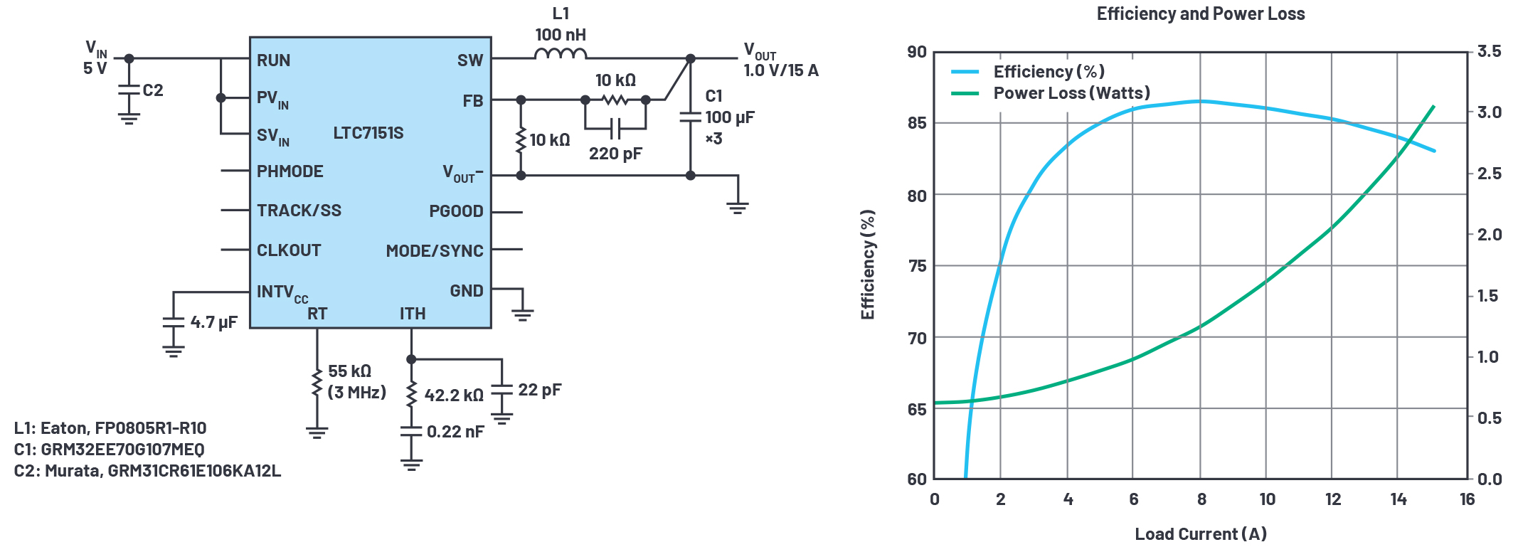
Figure 3: Schematic and efficiency for 5.0V input to 1.0V/15A with fSW = 3MHz
Figure 3 shows a 5.0 to 1.0V solution operating at a 3MHz switching frequency. A small size 100nH inductor from Eaton together with three 100µF/1210 ceramic capacitors delivers a low profile for FPGA and microprocessor applications. The temperature rise at room temperature is about 15°C at full load.
EMI performance
Meeting published EMI specifications—such as CISPR 22/CISPR 32 conducted and radiated EMI peak limits—with a 15A application could mean trade-offs in size, total efficiency, reliability, and complexity. Traditional approaches control the EMI by slowing down switching edges and/or lowering the switching frequency, which can reduce efficiency, increase minimum on and off times and increase solution size. EMI mitigation, such as complicated and bulky EMI filters or metal shielding, add costs in terms of board space, components and assembly and complicate thermal management and testing.
The proprietary Silent Switcher 2 architecture reduces EMI with integrated hot-loop capacitors, to minimise noisy antenna size. The LTC7151S keeps EMI low by incorporating MOSFETs and drivers which allows the IC designer to produce a device with built-in minimised switch-node ringing. The energy stored in the hot loop is highly controlled, even when switching edges have high slew rates, for EMI performance while minimising the AC switching losses at high operating frequencies.
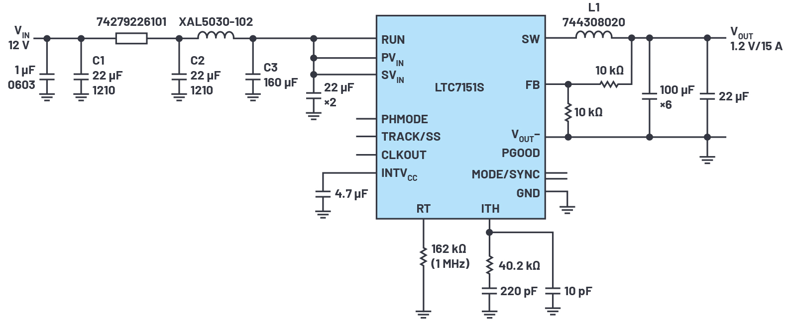 Figure 4: Schematic of a 1.2V regulator with 1MHz switching frequency
The LTC7151S has been tested in an EMI testing chamber and passed the CISPR 22/CISPR 32 conducted and radiated EMI peak limit with a simple EMI filter in front. Figure 4 shows the schematic of a 1MHz, 1.2V/15A circuit. Figure 5 shows the radiated EMI CISPR 22 test result in GHz transverse electromagnetic (GTEM) cell.
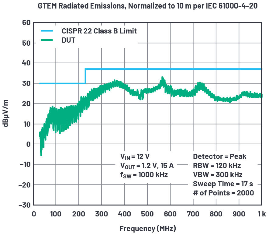
Figure 5: Radiated EMI in GTEM passes the CISPR 22 Class B limit
The proliferation of intelligent electronics, automation, and sensors in industry and automotive environments has driven up the required number and performance requirements of power supplies. Low EMI, in particular, has increased in priority as a key consideration for power supply design. An integrated regulator that meets stringent EMI demands addresses efficiency, thermal proficiency, robustness and size criteria for existing and emerging applications.
Product Spotlight
APV1111GVY
Panasonic

Panasonic PhotoMOS® Photovoltaic MOSFET High-Power Drivers
| SKU: | |
|---|---|
| Stock: | 3490 |
| Cost: | $3.95 |
