
A low cost Fly-Buck converter for 12V applications
The Fly-Buck converter has gained attention recently as an effective means to provide an isolated voltage rail. Many useful design notes exist and applications examples use Texas Instruments (TI) Constant On-Time (COT) ICs to provide one or more isolated rails for Programmable Logic Controller (PLC) isolated power, multiple isolated IGBT gate driver power rails, isolated RS485 interfaces and numerous other applications. Dan Tooth, Senior Field Applications Engineer, Texas Instruments explains.
Applications having a 12V intermediate voltage rail available are commonplace, such as smart meters, and some types require an isolated 5V output voltage. Also commonplace in all types of systems is the requirement for a non-isolated 3.3V rail to power the microcontroller and other 3.3V loads. In this article, the Fly-Buck from Texas Instruments provides both rails – a tightly regulated 3.3V rail and an isolated 5V.
The Fly-Buck is essentially a buck converter, with an additional winding(s) on the inductor to make a coupled inductor(s). Energy is transferred from the primary inductance and output capacitance to the secondary side during the converter’s off-time, when the high side IC MOSFET is off. The non-isolated output is tightly regulated by the controller IC and is called the primary output and the secondary (isolated) output voltage is set by the turns ratio minus losses.
Compared to the Flyback (or Buck) it is expected to see lower levels of EMI when using the Fly-Buck, assuming the PCB layout is good. For applications having sensitive communications sub-systems then an isolated converter with lower EMI is a major advantage. Other reasons to prefer the Fly-Buck instead of the Flyback or Push-Pull in certain applications have already been discussed.
For intermediate voltage rails of 3 to 5V then TPS55010 can be used. For higher voltages then the LM25017 / 18 / 19 (rated 48V) or the LM5017 / 18 / 19 or LM5161 (rated 100V) or LM5060 / 60A (rated 65V) are often used in Fly-Buck applications. LMR23630AF (rated 36V) can also be used.
The 12V Fly-Buck application
For low cost 12V applications, the TPS562219 and TPS563219 are 2A and 3A rated devices, with a Vin(max) of 17V, adjustable soft-start and a ‘power good’ output. Their control topology is a TI adaptive COT called DCAP2. This is a proprietary hysteretic-type control and generates its own internal ripple voltage ramp to emulate the output voltage ripple, enabling the use of all-ceramic output capacitors.
This integration keeps the design complexity and component count low, as the external RC2 ripple injection circuit is now not required. The switching frequency is pseudo-constant at 650kHz and the datasheet gives the recommended inductance to be used and range of output capacitance, both of which should be adhered to. The typical inductance to be used with these ICs is in the range of 1.5µH to 4.7µH, which will enable a compact magnetics solution.
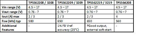 For higher power applications, the 4A rated TPS564208 can be used, see Figure 1 (above). These ICs allow for current sinking into the low side MOSFET, which is necessary as the current in the primary inductor typically reverses during the off-time in a Fly-Buck. A safe minimum negative current limit to use is -0.75A. Whether or not the current does reverse depends on the relative loads of the primary and secondary – a high primary load relative to the secondary will keep the current positive. The IC also has a positive current limit on the high side MOSFET and this is sensing the valley current rather than the peak. The negative current limit is likely to be the limiting factor in a design, which is the limit encountered as the secondary load increases. In Figure 3 (below) the peak negative current is -0.15A.
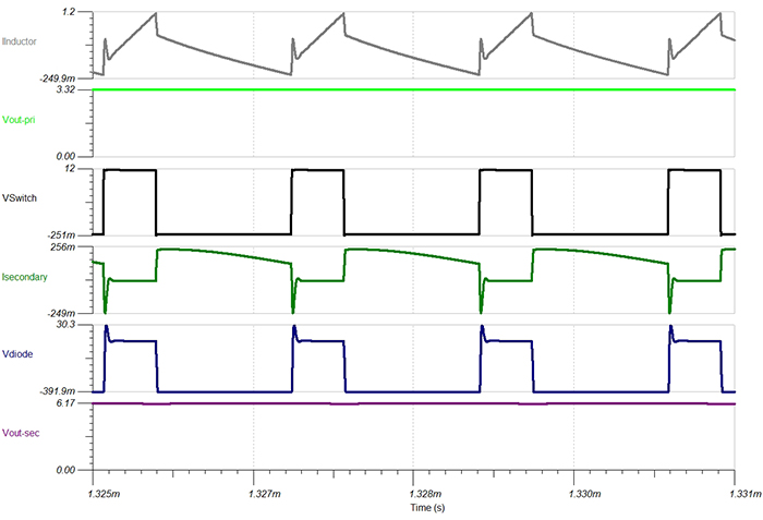
Figure 2 (below) shows the Fly-Buck converter application circuit. Vin is 12V(typ) and the goal is to regulate 3.3V on the primary and 5V on the secondary, after the low drop-out linear regulator (LDO). The primary duty cycle (D) is ~ 3.3 / 12 = 0.28 and it is desirable to keep D < 0.5 or 0.6 in Fly-Buck designs.
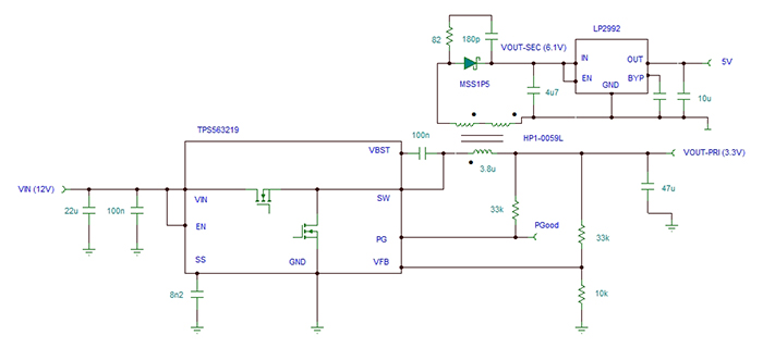
The coupled inductor used (Coilcraft HP1-0059) is a flexible, six-winding type that can be configured in many different ways. A 1:2 turns ratio is desired here and using the flexible inductor, this was achieved by connecting four of its windings in parallel (simply to obtain lower winding resistance) to form the primary and the remaining two windings are connected in series to form the secondary.
The inductance of each winding is 3.8µH. Other configurations are readily possible using this coupled inductor, e.g. obtain a bipolar +/-Vout by using 2+2 windings in series for the secondaries and the remaining two windings would be placed in parallel for the primary. It is important that the leakage inductance should be made as small as possible especially since the switching frequency of these ICs is relatively high, which means the time available to transfer the energy to the secondary is relatively short.
The secondary output voltage of Figure 2 is twice the primary output, minus the secondary diode drop and resistive winding losses, which gives 6.17V with 140mA secondary load applied. This can be post regulated using LDOs like LP2992 or TPS709. If the load on the secondary can be zero, then a pre-load resistor is advised to dissipate the leakage inductance energy.
The secondary diode experiences a reverse voltage equal to the input voltage multiplied by the turns ratio i.e. Vin.Ns/Np, plus a parasitic spike. For Ns/Np = 2 and Vin = 13V(max) then a 50V rated diode is reasonable, dependent on the spike magnitude. When the high side MOSFET in the IC turns on, the secondary diode doesn’t block instantaneously and a momentary reverse current is drawn through its capacitance, which oscillates with the stray circuit inductance and produces an oscillating diode voltage and current.
An RC snubber can be added around the diode to damp the oscillation and reduce the magnitude of the voltage spike across it. Note that not all Schottky diodes have low capacitance. The MSS1P5 low capacitance 50V Schottky with an 82Ω plus 180pF snubber across it worked well in the simulation.
Simulation and results
A TINA-TI simulation was performed by importing an exported simulation from Webench. The diode can be modelled by importing the manufacturer’s PSpice model into TINA-TI. The coupled inductor is modelled assuming a coupling factor of 0.98. The simulation waveforms are shown in Figure 3. The primary switch node voltage is clean as expected. There is a damped (snubbed) spike on the diode voltage / current.
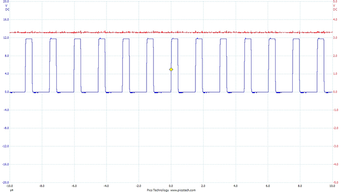
Testing was carried out without the post LDO regulator. Figure 4 (above) shows the switch node waveform, switching at 663kHz and the primary Vout, measured at 3.29V. The load is 10Ω on the primary and 44Ω on the secondary.
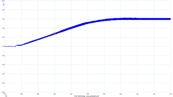
Figure 5 (below) shows the start-up waveform of the secondary, which is measured at 6.1V. A low cost IC can be used for 12V Fly-Buck applications, giving a simple design and low component count.

Product Spotlight
APV1111GVY
Panasonic

Panasonic PhotoMOS® Photovoltaic MOSFET High-Power Drivers
| SKU: | |
|---|---|
| Stock: | 3490 |
| Cost: | $3.95 |
