
Protecting circuits from ESD and other power surges
Protecting circuits from electrostatic discharge and other power surges is becoming more difficult with smaller chip geometries. Steve Rogerson looks at how the industry is coping.
As chip geometries shrink they become more susceptible to unwanted signals but there is less room on the die to install protection, putting more pressure on the system-level designers. On top of that, manufacturers of mobile electronics products, such as smartphones and tablets, are striving for more reliability in what is an extremely competitive field, but they want that reliability without drastically increasing costs.
These factors have led to the manufacturers of circuit protection products to delve deeper into the technologies, and they are having success: “Circuit protection has always been needed,” said Edgardo Menendez, Field Application Engineer, AVX, “but it has not been implemented completely. It is now being implemented more and more because of the growing use of wireless.”
Other areas where circuit protection is becoming increasingly important include Automotive, because of the explosion in electronics use in vehicles, MilAero for similar reasons and Industrial because of the increasing use of sensors and automated control. “In industrial, there is a need for more connectivity and sensors and so on,” said Felix Corbett, Director of Supplier Marketing, TTI. “There is a need for more data and so a need for more protection. There is also more electronics being put into the passenger areas of aircraft.”
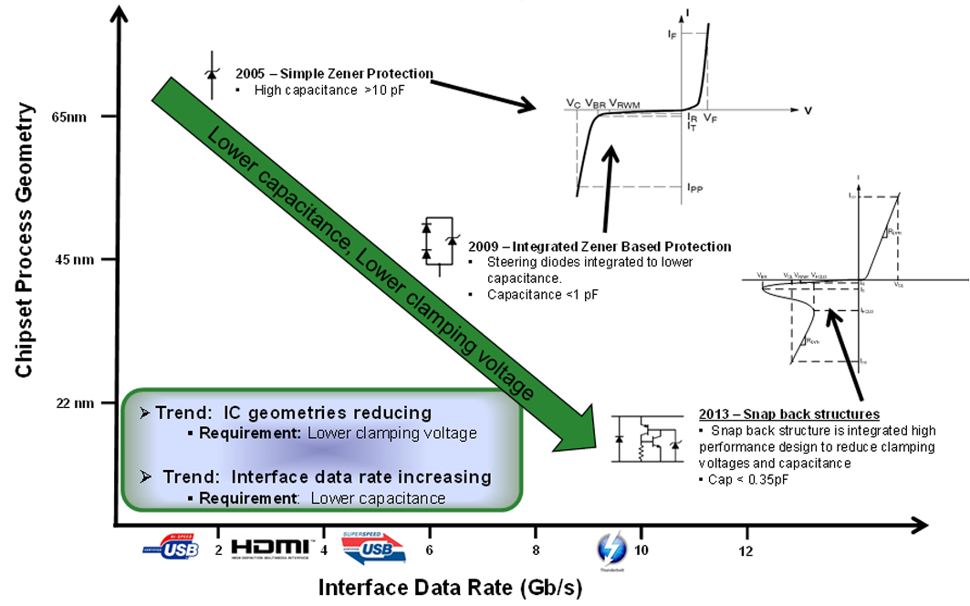
The latest Airbus, for example, is using more multimedia panels with larger screens even in the economy section and they have USB connectivity. “The user interface is the threat,” said Corbett. “On any of the USB ports you need protection against electrostatic discharge.” Traditionally, a TVS diode has been the most popular circuit protection device but it is rare that this a requirement and so manufacturers have looked for alternatives such as, for example, a multilayer varistor, popular in automotive and USB 3.0 applications. Varistors, diodes and the like are what are normally used, but one of the big challenges is keeping the capacitance low, below 0.5pF for varistors and down to the 0.2pF level for diodes. However, doing so can have negative effects on both breakdown and clamping voltages.

The latest Airbus provides more opportunities for passengers to connect, and that can be a threat
“When you go low in capacitance, other issues arise,” said Menendez. “Breakdown voltage goes up significantly. This is not such a bad issue because the IC can take pretty high energy and this is spread throughout the board. The IC can take a pretty high hit.”
But clamping voltages can go into the hundreds of volts range and many users want lower than this. This means a trade-off is needed between low capacitance and high clamping voltage.
Shrinking geometries
The reason for the low capacitance requirement comes from the shrinking geometries that result in a thinner oxide layer that is more sensitive to transient effects. “So you need some level of protection,” said Tim Puls, Product Marketing Manager, Semtech. “But the smaller size means it is more difficult for the manufacturer to put the same level of on-chip protection, so they need more off-chip protection, or system-level protection.”
Chad Marak, Director of Technical Marketing, Littelfuse, added: “The chips don’t have protection on the chip because it takes up too much room, so they leave all the protection off the chip and leave it up to us and others.” There is still some on-chip protection, but this is more to make sure the products survive the manufacturing environment rather than for their use in the outside world.
Higher data rates have also increased the need for circuit protection. The likes of USB 3.0 and HDMI are more prone to transient effects. But the diode used for protection has to have a working voltage that is low enough to be transparent to the data line. Once, 5V was acceptable but with faster data lines that became a barrier so it has dropped to 3.3 or even 2.5V. “As the data interfaces move to higher and higher speeds, what becomes the challenge is putting the protection on without distorting the signal,” said Puls. “That is why you need lower and lower capacitance. They also want a small form factor device, but size and capacitance move in opposite directions. So the trick is to get lower capacitance, smaller packing and maintain the same level of surge protection.”
Marak added: “There is a trade off. If your capacitance went down, the clamping voltage was made worse. Typically, the lower capacitance, the lower resistance so the clamping voltage was higher.” There has been a lot of research and development to get round this trade off and Marak admitted this had not been entirely successful: “There is still a lot of room to go but there has been a dramatic improvement,” he said. “Over the next few years, the push for lower capacitance will continue without damaging the clamping voltage.”
The difficulty is that the chip makers are also moving forward, as Lon Robinson, Product Marketing Manager, ON Semiconductor, pointed out: “With companies such as Intel adopting small geometries down to 22nm, that is a big jump and has created a lot of ESD issues,” he said. “The voltages went down and the sensitivity to ESD became greater. So we needed even lower clamping voltages. This left the industry in a bit of a pickle because the technology for protection wasn’t doing the job.”
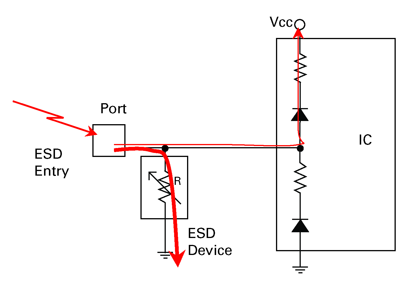
In an ideal situation all the current would go into the ESD device but to achieve this the resistance has to be as low as possible
A problem here, he said, was the IEC61000-4-2 standard, which does have a system level test for ESD but does not say how to apply that on a components level. “So we have to ask how to characterise our parts in a way that is relevant to a system level test,” said Robinson. Transmission line pulse (TLP) technology has become one way to deal with this. TLP can obtain current versus voltage curves in which each data point is obtained with a 100ns long pulse, with currents up to 40A.
“In the past, people had been looking at lighting style pulses, whereas we are trying to look at something much quicker,” said Robinson. “As we get to these fine geometries we have to look at this differently. TLP gives you something with the same rise time and the same energy. Basically, it gives you a way to zap your parts and see how your parts perform over the entire current range.” His colleague, compliance specialist Robert Ashton, added: “If you hit something with the IEC pulse, you can see if it survived or not. If it doesn’t survive, you don’t know what happened. With TLP, you can measure the voltage versus current and see the waveforms and other parameters such as dynamic resistance and so on. There is a whole host of things you know about your device that a few years ago you just didn’t know.”
More recent developments include a snapback structure in which the voltage will snap back to a lower voltage and then ramp up again helping to achieve the goal of low capacitance and low voltage. “This requires fine processing and complex design techniques,” said Robinson, “but it does give you a low clamping voltage at a low capacitance. And there is no downside to it. There is nothing but goodness for protecting circuits.”
Wireless
One answer with WiFi, smartphones or other wireless circuits is to put an RF inductor and a varistor together that can in effect provide lower capacitances at certain frequencies. Mobile wireless devices, though, face difficulties on two fronts, said Menendez - the charger and the antenna. “If you plug the power cord in to charge the phone and there is a surge caused by, say, a lighting strike, that can cause problems,” he said. “The other is high energy that could come in through the antenna.”
Technology trends for circuit protection
Tom France, Marketing Manager, Schneider Electric, thinks too much is being made of these problems: “The new smartphones basically act like a Faraday cage,” he said. “The charger could be affected. You could get an overvoltage that would cause the charger to fail, but it is doubtful whether that would get into the phone.”
As chip manufacturers produce smaller devices, the need for circuit protection increases but there is little room for the protection to be on chip as was once the case. This means engineers have to opt for better off-chip protection, but the characteristics of that protection are constantly moving. The result is an on-going engineering challenge to protect the latest devices.
Product Spotlight
APV1111GVY
Panasonic

Panasonic PhotoMOS® Photovoltaic MOSFET High-Power Drivers
| SKU: | |
|---|---|
| Stock: | 3490 |
| Cost: | $3.95 |
