Troubleshooting DDR3 memory interfaces
When designing circuits with DDR3 SDRAM modules, developers need solutions for checking the signal integrity on high-speed data lines. The new R&SRTO-K91/ R&SRTP-K91 oscilloscope option offers several tools - decoding of read and write cycles, display and analysis of eye patterns, and automated compliance testing for the DDR3, DDR3L and LPDDR3 standards.
The DDR3 standard was published in 2007 by the JEDEC consortium. DDR4 memory has been on the market for several years, and the DDR5 standard is being worked on intensively.
Nevertheless, DDR3 memory is still attractive for many applications because it costs less, is very reliable and compact, and offers high data volume as well as adequate data rates. For optimised power consumption, for example in mobile battery powered applications, versions conforming to the DDR3L and LPDDR3 standards are also available.
The DDR3 standard specifies memory components with data rates from 800Mbit/s to 2,133Mbit/s. These fast data rates are often new for industrial, medical and automotive applications, and the design and test requirements of the highly integrated electronic modules are demanding.
First of all, the memory components need a stable supply voltage that complies with the specified tolerances and does not pick up interfering signals from other functional units. Attention must also be given to the correct design of the memory interface signal lines, which have to support the high data rates. This includes, for example, an adequately dimensioned bandwidth over the entire transmission path (including the transitions at vias, connectors or relays), matching the line lengths of data and clock signals, and protecting lines with high data rates against crosstalk from other interfaces or functional units.
Finally, comprehensive test capabilities for evaluating the signal integrity and troubleshooting the DDR3 memory interface are indispensable when designing circuits.
Oscilloscopes are the first choice for measurements in this area because they offer many options for signal integrity testing, such as dynamic voltage and timing tests in line with JEDEC specifications (compliance tests) as well as the eye diagram test as an important analysis tool.
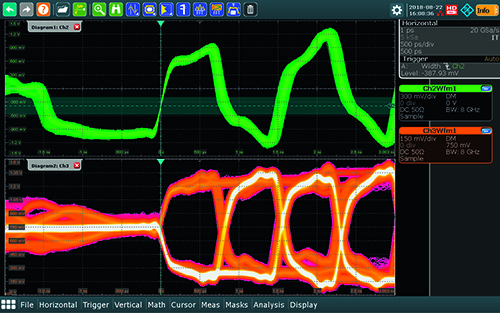
Above: Triggering on the read preamble with a negative pulse trigger
Eye diagram test
DDR3 interfaces use a parallel bus structure in which each set of eight single-ended data lines (DQ 0 to DQ 7) is clocked by a differential strobe signal (DQS). In the eye diagram of the individual DQ signals, the transmitted bits correspond to the rising and falling edges of the DQS clock signal.
The quality of many transmission parameters can be read from the eye diagram. For example, the eye opening time and jitter at the eye edges (bit transitions) can be seen on the horizontal axis, and the vertical eye opening and noise can be seen on the vertical axis.
The R&SRTO and R&SRTP oscilloscopes offer many analysis options for eye diagrams, including automatic eye diagram measurements, horizontal and vertical histograms for jitter and noise analysis, and masks for long-term stability tests. They acquire waveforms much faster than other oscilloscopes on the market, capturing several million bits within seconds and displaying them as an eye diagram.
To create eye diagrams from the bits of a long acquisition period, the R&SRTO-K91/R&SRTP-K91 DDR3 signal integrity debugging and compliance test software option provides the DDR eye diagram function. This software uses the edges of the DQS signal to break down the DQ signal into bits for the eye diagram display and offers numerous options for specific analyses, such as gate qualifiers and bit sequence filters.
In combination with the read/write decoding function, which is also part of the R&SRTO-K91/R&SRTP-K91 option and is described in more detail below, eye diagrams for read and/or write cycles can be displayed.
Targeted triggering on read and write cycles
The DDR3 data interface uses bidirectional lines for single-ended DQ data signals and differential DQS signals. To distinguish between read and write cycles, the edges of the DQ signal are transmitted with a different phase than the edges of the DQS signal. In the read cycle (when the memory sends data to the processor), the edges occur at the same time. In the write cycle (when the processor sends data to the memory), the DQ data edges are offset by half a bit width.
This clock offset, which is important for memory functionality, makes it difficult to display simple eye diagrams and measure time parameters such as setup&hold time. It is therefore necessary to observe read and write cycles separately in signal integrity analysis (see the application card ‘Triggering read and write cycles of DDR3 memories’). This is accomplished through targeted triggering on the start of the read and write cycles. The R&SRTO and R&SRTP offer many options for precise triggering. Their digital trigger system supports complex A-B-R trigger sequences (trigger events A, B and reset), and thanks to their digital architecture, they respond reliably to small signal changes and pulse widths <50ps.
The different preambles for the read and write cycles are a signal property of DDR3 memory interfaces that can be used for triggering.
For triggering on the negative read preamble, which is somewhat longer than one bit width, a correspondingly configured pulse trigger can be used. In the example on page 34, a negative pulse trigger >1ns was chosen for a DDR3 component with a data rate of 1,333Mbit/s (about 750ps bit width).
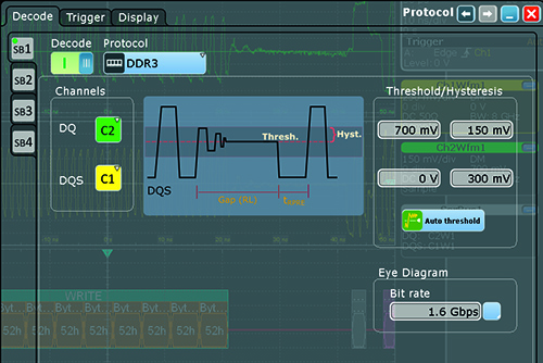
Above: Configuration of read/write decoding with the R&SRTO/R&SRTP-K91option
For triggering on write cycles, an A-B-R trigger sequence was defined that looks for write preambles (slightly larger than one bit width). In this example, the A trigger is set as a pulse width trigger with negative polarity and a width >2ns to find the start of write cycles. The B trigger is set to the positive pulse width of the write preamble (>750ps). If no valid B trigger event is found after an A trigger event, the R trigger (set to 2ns) resets the trigger system to search for A.
The R&SRTO-K91/R&SRTP-K91 zone trigger option offers another method for targeted triggering of read or write cycles. It allows the user to define zones that must be either passed through or avoided for valid triggering. The first zone in the DQS signal responds to the read preamble. The other two zones in the DQS and DQ signals target edges that occur at the same time.
Decoding of read write cycles
The R&SRTO-K91/R&SRTP-K91 option’s decoding function provides another way to detect read and write cycles. This function is selected from the protocol menu. It marks the read and write cycles within an acquisition of DQS and DQ signals based on the phase shift of the signal edges. The user simply selects the channel assigned to the DQ and DQS signals and then uses the Auto function to set the thresholds and hysteresis values.
As described in the eye diagram section, the DDR eye diagram function can use this decoding function. Another powerful tool is the eye stripe that marks mask violations in the time domain in red on the time axis and allows the user to use zoom coupling to conveniently navigate between mask violations.
Compliance tests for DDR3 standards
Compliance tests compare measured values with the specifications described in the standard. Powerful basic measurement functions such as setup&hold are helpful, but true convenience and efficiency can only be achieved with an automated solution. An automated solution provides detailed instructions for signal contacting, automatically configures the oscilloscope, acquires and measures the necessary waveforms, and issues a report with a summary of the results. The benefits increase when more measurements are required on different data lines and for different data cycles. R&SScopeSuite automatically solves the problem of separating the read and write cycles, and provides support for derating setup&hold measurements.
The R&SRTO/R&SRTP-K91 option does all of this. It checks DUTs for compliance with the DDR3 (JESD79-3), DDR3L (JESD79-3-1 and JESD79-3-1A.01) and LPDDR3 (JESD209-3C) standards. Using images and text, it conveniently guides the user through the measurements and indicates which channels of the oscilloscope should be connected and which measurement signals should be visible.
The results are presented in a way that gives the user a quick overview and also allows quick access to the details without having to generate a report.
Derating
The derating function determines a positive or negative adjustment of the measurement limit value based on the actual slew rate of the DQ and DQS signals. The slew rate is measured on the rising and falling edges of the DQS and DQ signals for each setup&hold measurement. The derating value is then determined by interpolating between the reference values defined in the JEDEC standard.
The slew rates of the DQS and DQ signals are shown together with the actual measured values. The resulting derating in this example is 50.226ps, which is taken into account in the tDS limit.
The R&SRTO/R&SRTP-K91 option automatically and efficiently performs measurements with derating. First it separates the cycles in the DDR3 signal into read and write cycles. Then it activates the relevant measurements over the defined signal time, graphically presents the results for the worst measured value, and summarises them in a report.
Timing tests
The JEDEC DDR3 standard divides the interface tests into timing tests and electrical tests. The timing tests contain specifications that describe the time behaviour of the individual signals. For example, the strobe timing defines the time response of the strobe signal to the clock and data signals. And the tRPRE timing measurement ensures that the read preamble is longer than 90% of a clock cycle. The start time of the preamble is approximated by linear interpolation of the falling strobe signal crossing zero. The end point is determined by the next time a rising edge of the strobe signal crosses zero.
Similar tests are required for other signals. Many of the measurements are similar, but not identical. The R&SRTO/R&SRTP-K91 option’s compliance tests cover all of the specified timing tests.
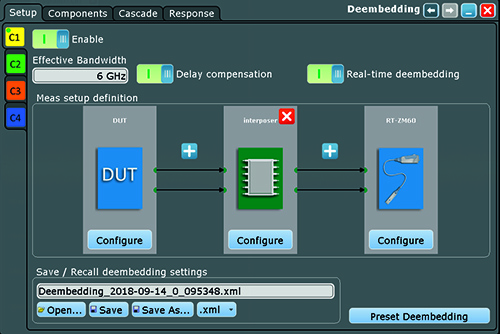
Above: Setup dialog for the deembedding function
Electrical tests
The electrical tests, as the name suggests, check the electrical properties of the signals. In the case of differential signals, the properties of the individual lines referenced to ground (V+, V–) are checked separately. Unlike the timing tests, only one signal is observed for these measurements. However, in some cases additional DQ and DQS signals are necessary to determine the read and write cycles
Contacting the test points
The JEDEC DDR3 specification refers to signals directly on the DRAM component, which is why the test points should be contacted as close as possible to the memory component during troubleshooting and signal integrity tests.
DDR3 memory components usually have a ball grid array (BGA) package and are either soldered directly on the PCB or on a dual inline memory module (DIMM). It is usually not possible to directly contact the balls on the underside of the package. With single-sided circuit boards or DIMMs, vias can be used to access the signal lines.
If contacting on the back of the board is not practical, it is possible to insert an interposer between the DIMM and the SDRAM component. The interposer feeds out specific signal lines for probe contacting. A DRAM component was unsoldered from the DIMM, and a raiser and an interposer were inserted between the DIMM substrate and the DRAM component.
Rohde & Schwarz offers modular wideband probes with numerous tip modules for signal contacting. For example, the R&SRT-ZMA10 solder-in tip module can be used to connect the probe to the test point. The R&SRT-ZMA40 browser tip module offers other flexible contact options.
As a general rule for all contact methods, the contacts should be kept as short as possible to minimise additional inductance and capacitance. For example, the solder contacts on the R&SRT-ZMA10 should not exceed two to three millimetres in length.
The multimode capability of the R&SRT-ZM modular probes provides great flexibility when measuring differential, single-ended or common-mode voltages. To measure differential signals such as the clock signal or DQS signal, the probe contacts the differential inputs VP and VN and ground. In multimode, it is then easy to switch between differential mode and single-ended mode for the electrical tests.
The best signal fidelity for the single-ended DDR data signals or control signals is obtained when the differential probe inputs (VP and VN) are used without additional ground contacts.
Deembedding compensates for transmission losses
Signal transmission through the probe (from the contact point of the DDR data line to the oscilloscope) is not perfect. The signal is distorted by transmission losses, making comparison with the specification more difficult. These losses are increased by additional test components such as interposers.
The R&SRTO and R&SRTP oscilloscopes support deembedding, which is the common method used to compensate for these transmission losses. The R&SRTO-K121/RTP-K121 deembedding option calculates a compensation filter based on S-parameters and applies it to the acquired waveforms. An S-parameter file describing the transmission characteristics can be loaded for each element. When deembedding is activated, the characteristics of the overall path (including the oscilloscope input) are determined once and a compensation filter is calculated.
With the R&SRTP-K122 option, hardware-accelerated deembedding can be performed in real time on an R&SRTP. The user can utilise the oscilloscope’s high acquisition rate of up to one million waveforms per second to quickly and reliably capture rare events during troubleshooting. The trigger system also benefits from real-time compensation since it acts on the compensated and therefore correct signal.
Summary
The integration of DDR3 memory devices presents circuit designers with very specific design and test challenges that can best be addressed with a customised, oscilloscope - based measurement solution. The R&SRTO-K91/R&SRTP-K91 option has all the necessary capabilities - functions for effective troubleshooting such as DDR3 eye diagrams and read/write decoding as well as conveniently guided standard compliance tests. The real-time deembedding function of the R&SRTP automatically eliminates distortion effects from the measurement setup, improving the reliability of analysis results and increasing the efficiency of measurements.

