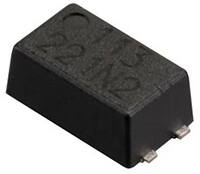
SPI FRAM comes in ultra small package
A new ultra small package for Fujitsu’s 1Mbit SPI FRAM device is available at distributor Rutronik as of now. It is the ideal solution for power critical miniature applications in sensor and wearable markets. This new miniature 8 pin wafer level chip scale package (WL-CSP) is an additional package variant to the existing product MB85RS1MT.
In comparison to the industry standard SO8-package, the new WL-CSP package (3.09x2.28x0.33mm) reduces the surface mounting area by 77%, and the device height by 80%. With this product release, Fujitsu is offering 1Mbit SPI FRAM product with the industry’s smallest packaging technology.
While conventional non-volatile memories like EEPROM or flash memory cover an endurance of the range of only 1 million write cycles, the MB85RS1MT FRAM device provides an endurance of 10 trillion read/write cycles, thus allowing a flexible storage of real time logging data.
It can be overwritten fast and flexibly into each memory cell without any waiting time, resulting in a much lower energy consumption in the writing access.
It also helps extending the battery lifetime, especially for wearable and sensor applications with frequent logging functions.
The MB85RS1MT device has an operating voltage range of 1.8V up to 3.6V and an operating temperature range of -40°C up to +85°C. It guarantees a data retention of 10 years at 85°C.


