
Driving up NAND flash capacities to support the data-driven future
Data is interwoven into the fabric of our lives, regardless of how much or little we personally interact with the digital world. Successful, reliable and long-term data storage ensures that everything, from massive data centres and AI platforms down to menial wireless sensors and even our kitchen appliances, continue to function around us. And it is flash silicon-based memory technology that is increasingly being chosen to make this possible.
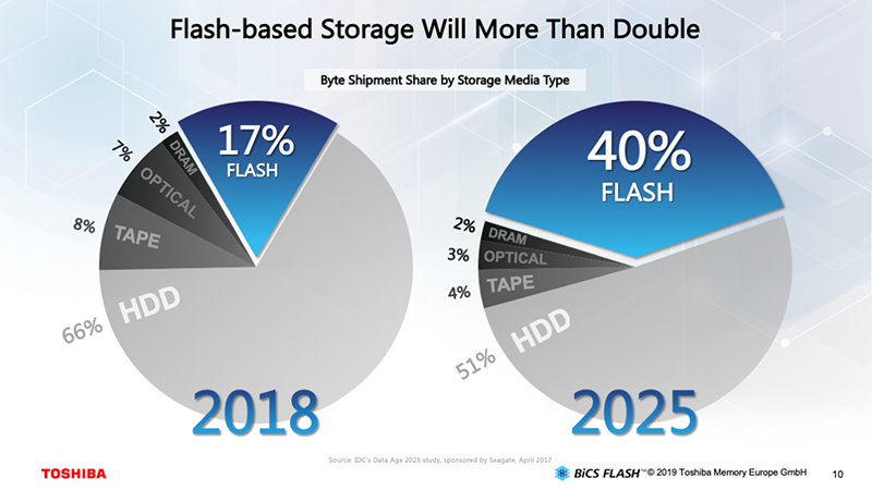
Taking a global perspective, it is true that spinning platter hard disk drives (HDD) continue to make up the greater portion of storage, making up around 66% of worldwide capacity in 2018. However, it is predicted that the share of global storage attributed to flash-based storage will grow significantly from 17% in 2018 to 40% in 2025, with HDDs share dropping to 51% (figure 1). In this timeframe it is predicted worldwide storage capacity will grow from 16ZB (zettabytes) today to around 163ZB.
Consumer products, such as smartphones, tablets and cameras, along with industrial equipment and sensors, automotive systems and medical devices, all rely upon flash memory, often integrated alongside their processors, that stores both data and the code they execute. However, data centres find attraction in flash memory due to its near real-time response to read/write requests, and high data transfer rate. As demand for massive data processing for artificial intelligence (AI) and machine learning applications grows, so interest in flash-based storage will evolve in tandem.
The invention of flash memory
Prior to the existence of flash memory, silicon-based memory data retention relied on it either being continually powered (volatile static random-access memory or SRAM) or could only be programmed and erased in its entirety using dedicated tools (non-volatile erasable programmable read-only memory or EPROM). The invention of flash memory changed this.
Now non-volatile silicon-based memory could be programmed in-situ and also be modified without requiring the removal of the chip itself or extra tools. Additionally, it could be integrated on-chip alongside other silicon devices, such as microprocessors, for storing program code and non-volatile data.
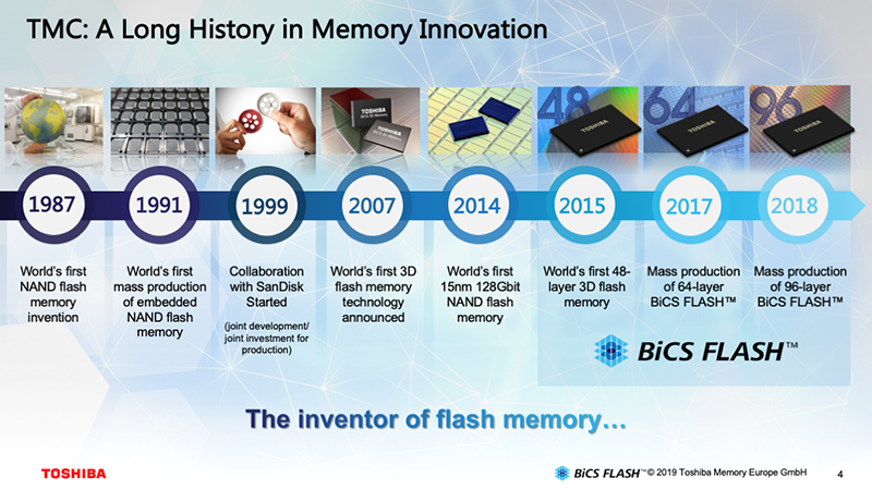
Flash technology was developed by engineers at Toshiba in 1984, leading to the creation of the first NAND flash memories in 1987 (figure 2). Each memory cell consisted of a floating-gate transistor capable of storing a single bit of data (single-level cell or SLC). As has been the case in other aspects of the semiconductor industry, regular moves to ever finer lithography following Moore’s Law initially enabled more cells, and thus data, to be packed onto a single die.
However, with today’s lithography reaching dimensions of just 12nm, the fine feature size poses physical challenges in reliably storing data in, and recalling data from, the memory cells. If the memory cells cannot be made smaller, other approaches are required to pack more data into the same space.
The only way is up
One approach to growing capacity using traditional lithographic approaches is to increase the quantity of data stored per memory cell. This led to multi-level cell (MLC) and triple-level cell (TLC) technologies storing more than one bit of data per cell, effectively doubling or tripling capacities for existing die sizes.
However, this approach to expanding storage has a disadvantage in that wear on the cells increases, resulting in reduced lifetime and durability. With a range of markets being serviced, suppliers could choose whether to provide high-capacity, low endurance and low-cost storage as is often suited to consumer applications, or higher endurance but higher cost storage, suited to computing, industrial and automotive applications where endurance is more of a concern.
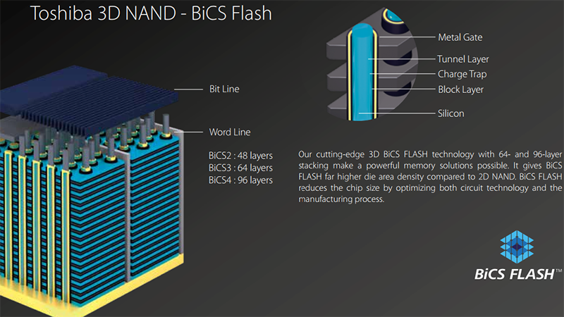
Ultimately more capacity requires more storage cells per die, but sticking to a single-layer, planar approach while relying on Moore’s law to solve the area issue was not going to deliver the solution. Instead, flash manufacturers have been moving into the third dimension, developing 3D approaches that generate flash memory which looks similar to a high-rise building, and this in ever-increasing numbers of layers (figure 3).
Next generation flash technology
Manufacturers such as Toshiba have made significant investments in flash technology with their 3D NAND BiCS (Bit Column Stacked) technology being introduced in 2007. Having initially started with a 48-layer approach, further development has grown this to 64 layers with BiCS3 and, most recently, 96 layers with BiCS4. Not only does the 3D approach deliver more capacity, it also results in higher data transfer speeds.
However, this advantage can quickly be lost again once the die is packaged due to the impact of the wire bonding. To resolve this challenge, new approaches had to be developed to improve die-to-package connectivity, resulting in Through Silicon Via (TSV) technology. This shortening in the electrical pathways delivers benefits in data transfer speeds and power savings as well as simplifying die-to-die bonding in stacked-die solutions.
The increase in available speed has also impacted the standardised interfacing technologies for both PCs and laptops, with NVMe slowly replacing SAS/SATA, and UFS growing in popularity over the traditional eMMC standard. A further quantum growth in storage capacity has been made possible with the introduction of quad-level cell storage (QFC), placing four bits in each cell. As a result, single package devices with 2.66TB of storage are now possible based upon the use of 16 stacked die, each of 1.33Tbit capacity. The first SSDs featuring BiCS4 flash include the client NVMe M.2 XG6 series as well as the BG4 series of single BGA packed devices.
Aggregating flash storage in data centres
Although SSDs can deliver significant performance improvements over alternative storage media, they are still coupled with a significant capital expenditure. With this in mind, Toshiba has been developing a software solution that enables data centres the ability to maximise usage of this high-value resource with minimal overhead.
Traditionally, the direct attached storage (DAS) binds the selected storage to server hardware. This typically results in servers whose CPUs are underutilised, or whose storage is not used to full capacity.
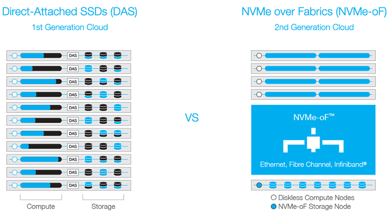
With the widespread use of high-speed, low-latency networking technology, it is possible to disaggregate storage and CPU. This enables the creation of a pool of SSD-based high-speed storage that is available for use by a collection of high-performance processing hardware. The approach, known as NVMe over Fabrics (NVMe-oF) is delivered by the software KumoScale (figure 4). The result is an optimal allocation of storage capacity and performance at each node, with the shared NVMe resource delivering DAS-like performance.
Conclusion
It is incredible to see how flash technology has impacted our lives in little more than a generation. From massive computing platforms, to humble, light-weight and compact sensors, flash memory has provided, and continues to provide, durable, low-power, high-speed storage that is suited to a mass of applications.
Furthermore, with the continued investment and research being undertaken by suppliers such as Toshiba, consumers will continue to see the benefits that result from advances in flash memory technology in their smartphones and computers, as well as indirectly through cloud services and machine learning technologies.
Product Spotlight
APV1111GVY
Panasonic

Panasonic PhotoMOS® Photovoltaic MOSFET High-Power Drivers
| SKU: | |
|---|---|
| Stock: | 3490 |
| Cost: | $3.95 |
