
Power management challenges for wearable technology
The field of wearable technology is expanding rapidly but still faces challenges in power management. By Lauren Ofstedahl, Corporate Communications and Business Development Manager, Dialog Semiconductor.
Even though the portable equipment sector has increased rapidly over recent years, growth is expected to explode in the near future with a boom in Wearable Devices and the Internet of Things, which envisions more than 50bn devices wirelessly connected to the internet in the next few years. Wearables and the Internet of Things introduce a whole new category of wirelessly-connected digital ‘accessories’. The wireless communications architecture of those accessories typically consists of a short-range, low data rate and low power sensor node that periodically transmits data to a remote hub such as a cell phone or application specific device. Examples include health and well-being monitoring devices like FitBit and the Nike+; mobile phone accessories and companion devices such as smart watches; and various monitoring and control products such as proximity sensors and high-end remote controllers (Figure 1).
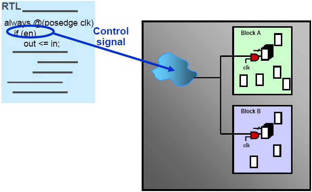
Figure 1 - Silicon and block level clock gating
Developers of such technology face pressure constraints including miniaturisation, low power and low cost, and semiconductor manufacturers are addressing these points by building increasingly efficient components. Nevertheless, there are still important decisions to be taken around wireless standards if the widely predicted 50bn wireless connections is to be realised by 2020. This new architecture imposes an increasing demand for high-performance, battery-operated and/or energy harvesting powered, SoCs in communication devices, shifting the focus from traditional constraints (such as footprint, performance, cost and reliability) to power consumption. Designers of portable equipment using coin cell, alkaline batteries or energy harvesting are challenged by system level energy budget considerations, mainly driven by MCU and RF current consumption, as well as the need for small size limiting the size of the battery or energy harvester. When designing a battery powered wireless product, the effect of power draw is critical to the success and longevity of the product.
Smart sensor nodes
Developers of wireless devices for Internet of Things have a plethora of radio communications protocols to choose from. Some applications, especially those that do not need to be interoperable, are based on the development of bespoke protocols optimised to minimise current consumption, latency, connection time as an example. However, over the past decade several standard low power protocols that address many of these requirements have become established in the marketplace. Popular standards for sensor nodes are WiFi, ZigBee (RF4CE), Ant (Ant+), Bluetooth and Bluetooth Smart (BLE). Many of these standards also have the very real advantage that consumer devices such as cell phones increasingly support them, providing a ready supply of suitable ‘hub’ devices for connecting to the internet.
Bluetooth Smart was adopted by the Bluetooth SIG in 2007. The purpose of this technology is to enable power sensitive devices to be permanently connected to the Internet. Typically Bluetooth Smart sensor devices are required to operate for many years without requiring a new battery.
This technology is primarily aimed at mobile telephones, where it is envisaged that a star network topology, similar to Bluetooth, will be created between the phone and an ecosystem of other devices. Among its features are a new advertising mechanism for easy discovery and connection, and an asynchronous contactless MAC for fast, low-latency transactions.
Bluetooth Smart is also known as Bluetooth v4.0 or v4.1 and is part of the public Bluetooth specification. As a result of being a standard, Bluetooth Smart benefits from all the advantages of conformance and extensive interoperability testing at ‘unplug-fests’. Most new Bluetooth chipsets from leading Bluetooth silicon manufacturers support Bluetooth and the new Bluetooth Smart functionality.
Established in 2004 by the sensor company Dynastream, ANT is a low power proprietary wireless technology which operates in the 2.4GHz spectrum and usually operates from a coin cell. Typically, the ANT transceiver device is treated as a black box and its primary goal is to allow sports and fitness sensors to communicate with a display unit, for example a watch or cycle computer. ANT+ has taken the ANT protocol and made the devices interoperable in a managed network, thereby guaranteeing that all ANT+ branded devices work seamlessly. Similar to Bluetooth Smart, ANT devices may operate for years on a coin cell. ANT devices are not subject to the extensive conformance and interoperability testing applied to other standardised technologies; ANT+ introduced a new certification process in 2011 which is chargeable and a prerequisite for using ANT+ branding.
Based on the Institute of Electrical and Electronics Engineers (IEEE) Standard 802.15.4-2003, ZigBee is a low power wireless specification established in 2002. It introduced mesh networking to the low power wireless space and is targeted at applications such as smart meters, home automation and remote control units. ZigBee is not a frequency hopping technology. It therefore requires careful planning during deployment to ensure there are no interfering signals in the vicinity. Unfortunately, ZigBee's complexity and power requirements do not make it particularly suitable for maintenance-free devices that need to operate for extensive periods from a limited power source. Radio Frequency for Consumer Electronics (RF4CE) is based on ZigBee and was standardised in 2009. RF4CE's intended use is as a device remote control system, for example for television set-top boxes. The intention is that it overcomes the common problems associated with infrared: interoperability, line-of-sight and limited enhanced features.
Although WiFi is a very efficient wireless technology, it is optimised for large data transfer using high-speed throughput and is not really suitable for coin cell operation. Some companies are attempting to use WiFi for sensor devices. However, special proprietary driver software is required and only limited functionality can be achieved. From the above comparison we see that, with the exception of WiFi which cannot operate on coin-cell batteries due to its peak current requirement, the most power efficient technology is Bluetooth Smart. Bluetooth Smart also provides very good peak current and very low latency, fully covering the requirements of coin-cell powered sensor nodes. In another comparison of the coin-cell targeted protocols, ANT, ZigBee and Bluetooth Smart in cyclic sleep node scenarios, it is again shown that Bluetooth Smart achieves the lowest power consumption, followed by ZigBee and ANT.
Ultra low power
Bluetooth Smart appears to be the most power-efficient wireless standard suited to the growth of the market in Wearables and the Internet of Things. However, is it enough just to achieve ultra low power requirements in wireless sensor nodes? Obviously the answer is no, as the sensor design should be supported by advanced power saving techniques to achieve this goal. Dialog’s DA14580 chip is a Bluetooth Smart controller that combines all known power saving techniques to achieve unprecedented power consumption, using a number of techniques.
Clock gaters are usually special cells supported by a technology library that are inserted into the logic to disable clock of register cells when not enabled. Silicon clock gating is the automatic insertion of clock gaters at chip synthesis and includes clock gating inference and clock gater decloning (push gating into higher hierarchy) / re-cloning where necessary. Functional clock gating is clock gating at block level in order to disable the blocks that don’t need to be clocked at specific time frames, depending on the functionality. The DA14580 combines both techniques for minimising active clock cells (Figure 1).
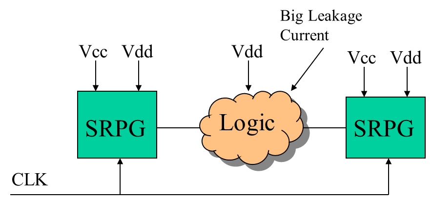
Figure 2 - Power gating
Power gating is a technique to enable electrical isolation of a whole power domain. In the example shown Figure 2, the VDD power domain can be shut-off and VDDC reduced to retention voltage by using special State-Retention Registers with Power Gating (SRPGs). The DA14580 includes different LDOs per power domain (independently controlled) and power islands that are controlled by power switches and are isolated by retention cells. The power gating technique can reduce the power of a specific power island up to 10 times, because the whole domain can shut-down and is combined with high-Vt standard cell selection for minimum leakage. On top of the above techniques, DA14580 can also support variable voltage supply with retention LDO trimming which is used to lower the voltage based on system load; using this technique the system can select the lowest frequency needed to execute a specific action. Dividers on the main clock, a low power clock option (32kHz) and ultra-low power option with internal RCX (10.5kHz) are also included. Moreover, the DA14580 includes various software low power modes that automatically switch off parts of the design that are not required, depending on the application, such as extended sleep (with full system RAM retained), and deep sleep.
From an RF point of view, the application of high quality on-chip inductors which operate at the highest possible impedance level, coupled with current re-use techniques in high-frequency part Class-D RFPA, deliver optimum efficiency while keeping the harmonic distortion well below the spectral mask. State-of-the-art circuit design techniques have also been used on all other radio blocks. Combining all the above techniques, DA14580 demonstrates impressive power consumption figures: deep sleep of 0.5µA (only retention memory maintained); extended sleep of 1.2µA (all system memory maintained); Tx of 4.8mA at 3V, and Rx of 5.1mA at 3V. In a typical application like proximity these numbers lead to a lifetime of four or more years for a connection interval of four seconds with a coin cell battery of 225mAh. Moreover, these power consumption figures allow ambient energy harvesting techniques as in the iBeacon reference design in Figure 3.
![]()
Figure 3 - Energy harvesting iBeacon reference design
The success of the Wearables Market and the Internet of Things will depend significantly on the ability to design sensor nodes that operate on coin-cell batteries or energy harvesters for long periods of time. To achieve that requires a power efficient wireless protocol, supported by the latest technological advancements. Dialog’s DA14580 combines all the above characteristics into a single chip, that is already able to demonstrate power consumption figures that match the requirements of the Wearables Market and the Internet of Things.
Product Spotlight
APV1111GVY
Panasonic

Panasonic PhotoMOS® Photovoltaic MOSFET High-Power Drivers
| SKU: | |
|---|---|
| Stock: | 3490 |
| Cost: | $3.95 |
