Power
Vishay Siliconix Released Asymmetric Dual TrenchFET Power MOSFET in PowerPAIR 6 mm by 3.7 mm Package
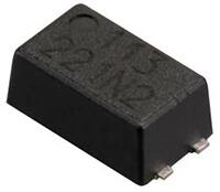
Vishay has introduced the first asymmetric dual TrenchFET power MOSFET in the PowerPAIR 6 mm by 3.7 mm package to utilize TrenchFET Gen III technology, reducing on-resistance by 43 % when compared to previous-generation devices, while offering higher maximum current and enabling increased efficiency. Offering the industry's lowest on-resistance for this device type, the SiZ710DT combines a low- and high-side MOSFET in one compact device, saving space over using two discrete solutions in dc-to-dc converters.
BefoIn addition, replacing SO-8 devices in lower-current and lower-voltage applications can increase efficiency. A single PowerPAK 1212-8 or SO-8 has on-resistance down to the 5 mΩ or 4 mΩ range, respectively. However, the low-side Channel 2 MOSFET of the SiZ710DT utilizes the optimized space from the asymmetric structure and offers a lower on-resistance of 3.3 mΩ at 10 V and 4.3 mΩ at 4.5 V, and a maximum current of 30 A at + 25 °C and 24 A at + 70 °C. In addition, the high-side Channel 1 MOSFET features an improved on-resistance of 6.8 mΩ at 10 V and 9.0 mΩ at 4.5 V.
By having the two MOSFETs already connected inside the PowerPAIR package, layouts are made easier and parasitic inductance from PCB traces are reduced, increasing efficiency. In addition, the SiZ710DT's pinning is arranged so that the input is on one side and the output is on the other, further simplifying the layout and saving PCB space.
The device is 100 % Rg and UIS tested, compliant to RoHS directive 2002/95/EC, and halogen-free according to IEC 61249-2-21.


