
Use circuit models to chart power device thermal parameters
Higher power levels are being handled in smaller spaces meaning that remaining losses are concentrated in the same small area or volume. Thermal considerations can be the critical path to a successful design, says Kim Mosley, Vicor
Continuous progress in semiconductor device performance is matched with more efficient circuit architectures, and with ingenious physical constructions allowing more performance into smaller modules. Switching architectures have long been the norm for all but niche, lower-power regulator designs, and each new generation of power transistors edges closer to the ideal switching behaviour of providing zero conduction losses and zero switching losses.
In systems where cooling is not appropriately designed, thermal limitations may be more stringent than electrical limitations. Components may meet datasheet limits on operating temperature before those of, say, output current. Thermal considerations can be the critical path to a successful design.
Cooler devices live longer
Engineers will always strive to manage the thermal aspects of the design to keep the operating temperature of vital components as low as possible. Predicting thermal behaviour at the design stage is not necessarily a simple task, not least because, under today's SWaP (size, weight and power) objectives, the option of attaching an ample heatsink is often not available.
The established, key parameter in any thermal calculation is the junction temperature (Tj). Between it and the external ambient thermal environment there will be numerous complex structures that present barriers to heat flow, or a series of paths by which the heat can escape. As well as wire bonds to aid heat conduction and layers of mould material to impede it, there may be multiple sources of heat, with heat generated at a specific location as well as from neighbouring components. Even the location of the maximum temperature rise may change, when the device is operated under different input voltages, different output voltages, and different cooling strategies.
The thermal resistance of copper, and most electrical components, increases with temperature, adding an incentive to keep temperatures low. As the temperature increases, electrical resistances increase, and heat losses are, proportionately, greater. Techniques to model maximum internal temperature of these structures typically employ finite element modelling and computational fluid dynamics, rather than quick, everyday calculations.
Simplified thermal models
An alternative strategy exists, in the form of thermal models presented in electrical-analogue terms. These thermal models are composed of resistors, current sources and voltage sources. Applying the same analysis as in the electrical domain offers a simple means of quantifying the maximum internal temperature and the heat flow through the various cooling paths in the design.
These thermal models use the concept of a single virtual node that represents the maximum internal temperature of an active device or module. The virtual node does not represent a fixed location in the device, but the maximum internal temperature of the device under all electrical and thermal cooling conditions. Around it are arrayed representations of each of the paths by which heat can flow away from that node. In this analogy, the resistor symbol represents such a path (offering some restriction to heat flow) and has units of degrees Celsius/Watt (C/W). The heat source can be determined from datasheet graphs showing device efficiency or power dissipation (W) at known electrical operating conditions. In this steady-state operation, power dissipation must be equal to the heat conducted from the device to the environment. In the thermal-electrical analogy, the power loss in the thermal system is represented in the electrical circuit model by a current source applied to the internal virtual thermal node. The paths for heat conduction to the environment typically include conduction through the top surface of a package, conduction via the device's pins or pads to the PCB, or conduction through the bottom of a package.
In steady-state, a stable temperature will exist at each of those boundaries, to a heatsink, coldplate, or to the surface of the PCB. This fixed temperature in the thermal system is analogous to a voltage source in the electrical system. It remains at the same value (in degrees C) even as it absorbs whatever heat flows into it.
Underpinning this is a detailed, finite-element computation simplified to what is, in effect, a behavioural model for the thermal performance of the device in its package. A simple calculation shows how the models are applied.
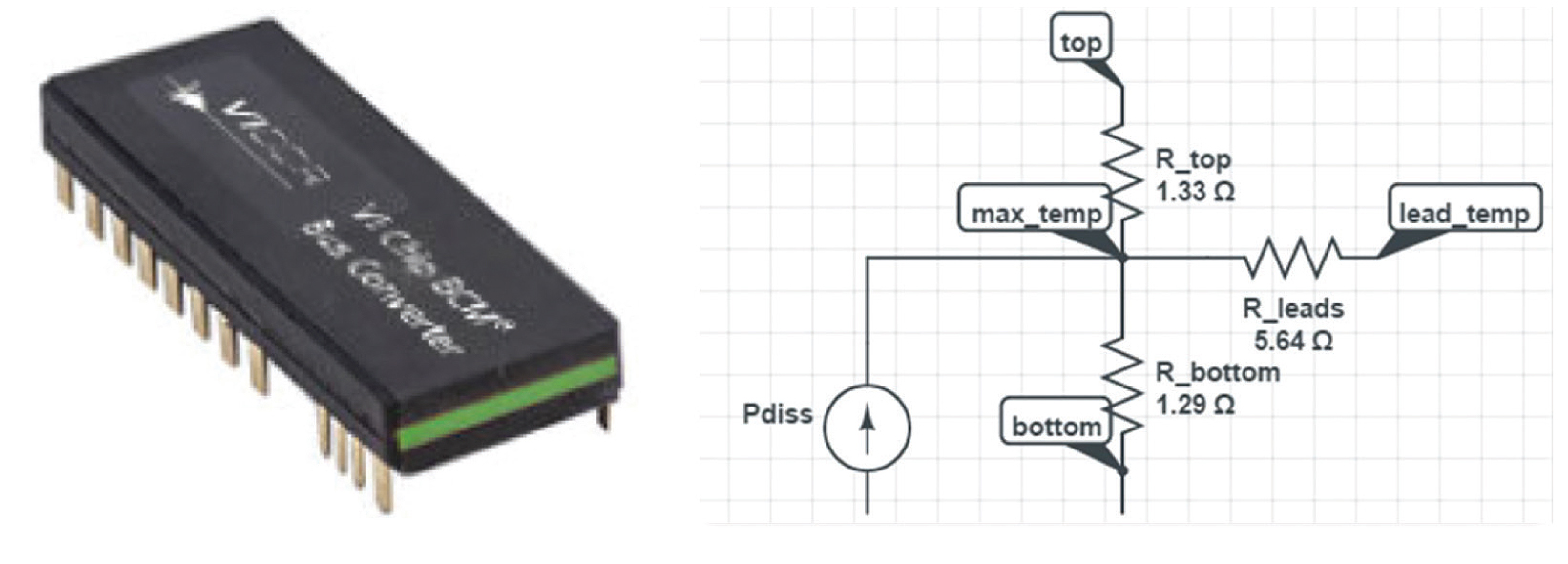 Figure 1: Simplified model of a BCM (bus converter module)
Figure 1 shows the simplified model of a BCM (bus converter module) in Vicor's ChiP package. The BCM is a fixed-ratio DC/DC converter that can be employed as a DC transformer to transpose one bus voltage to another. The ChiP is an IC-style, dual-in-line, fully-over moulded package. The BCM occupies a small package, delivers substantial amounts of power and benefits from good thermal design to remove the dissipated heat.
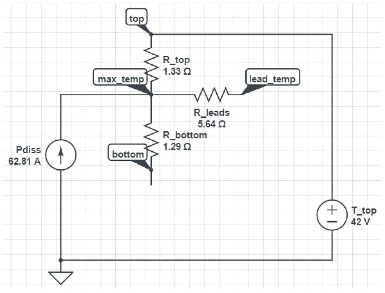 Figure 2: BCM ChiP with top coldplate cooling
Figure 2 shows the simplified thermal model of a BCM, in use. In this scenario, the device delivers 1750W at an efficiency of 96.5%, for a power dissipation value of 62.81W. Dissipated power is shown as the thermal model current source. Three possible paths to extract heat are shown, i.e through the moulding to the top surface, through the moulding to the bottom, and via the leads/pins into the PCB. Here, the bottom surface and the leads of the device are assumed to be adiabatic. In the case of the bottom surface, this could be because there is expected to be an air gap between it and the PCB and for the leads it could be because the PCB is expected to operate at a high enough temperature that there will not be enough of a temperature difference between the inside of the device and the PCB to create the potential for heat flow. The top surface of the device is assumed to be in contact with a heatsink or coldplate that maintains the top surface of the device to a temperature of 42°C. Based on these assumptions, the maximum temperature of the inside of the device can be estimated to be equal to the maximum operating temperature of 125°C.
Thermal interface material (TIM) provides thermal coupling between the converter and a coldplate or heatsink by filling surface irregularities with a material of much higher thermal conductivity than air. It may not be required to represent this added thermal resistance in the model as its thermal resistance is usually an order of magnitude less than the other resistance values in the thermal circuit model.
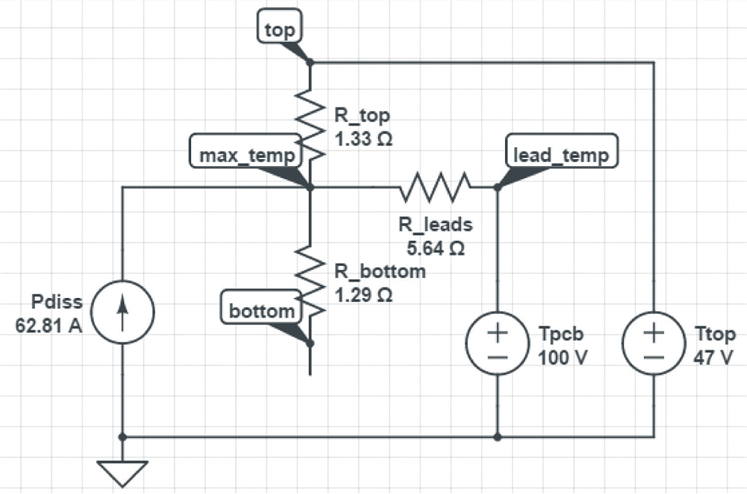 Figure 3: BCM ChiP with top coldplate cooling and PCB cooling added
In Figure 3, the designer has activated the cooling path via the converter's connecting pins, into the PCB where a heavy copper plane might be provided to act as a thermal path to the environment. In this case the designer would expect the PCB temperature to be 100°C. The normal rules of paralleled current paths (in the electrical view) continue to apply and are used to quantify the maximum internal temperature in the circuit. The top surface is now acceptable with 47°C rather than 42°C to keep the maximum internal temperature of the device below the 125°C maximum operating temperature. The circuit model also shows that 4.38W of the total 62.81W of power dissipation is conducted to the PCB under these conditions and the balance of 58.43W would be conducted through the top. Alternatively, making thermal contact to both top and bottom of the package with heatsinks or coldplates and keeping those surfaces at 84°C, as in Figure 4, would also keep the maximum internal temperature to 125°C. In this case the 30.93W of heat conduction through the top is almost equal to the 31.88W of heat conduction through the bottom.
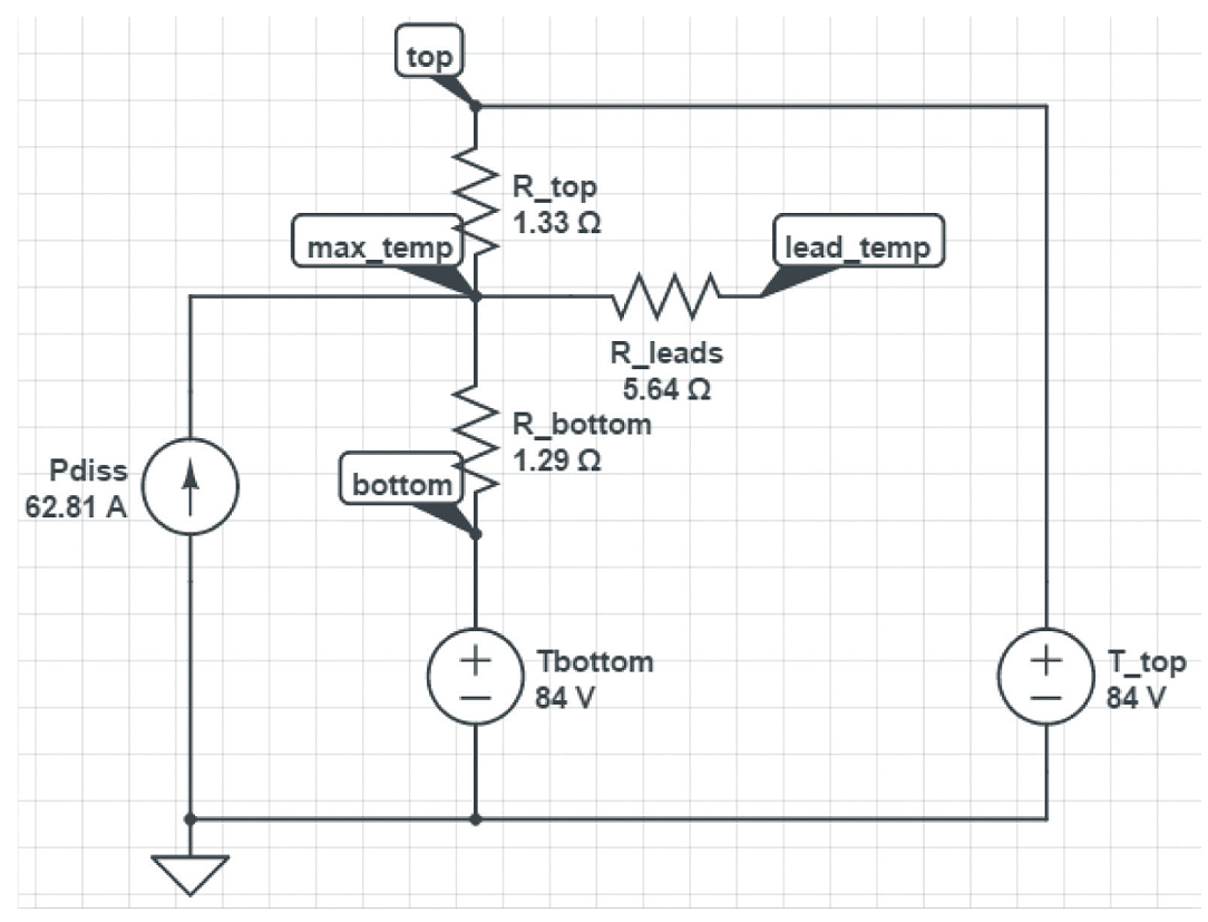 Figure 4: BCM ChiP with coldplate attached top and bottom
Adding airflow over a heatsink
Usually data is available that will allow the engineer to add the heatsink’s thermal behaviour to a circuit model. This heatsink performance is typically characterised as a graph of thermal resistance in °C/W as a function of air flow across the heatsink in linear feet/ minute (LFM). A polynomial fit to this curve also provides a mathematical function for calculating thermal resistance as a function of air flow. Figure 5 shows a thermal resistance graph for an 11mm Vicor heatsink (P/N 40704). The thermal resistance can be read from the graph and added directly into the thermal model as the analogous electrical resistance. The thermal resistance of the heatsink at an air flow of 400LFM can be read from the graph or calculated using the polynomial to be 2.1°C/W.
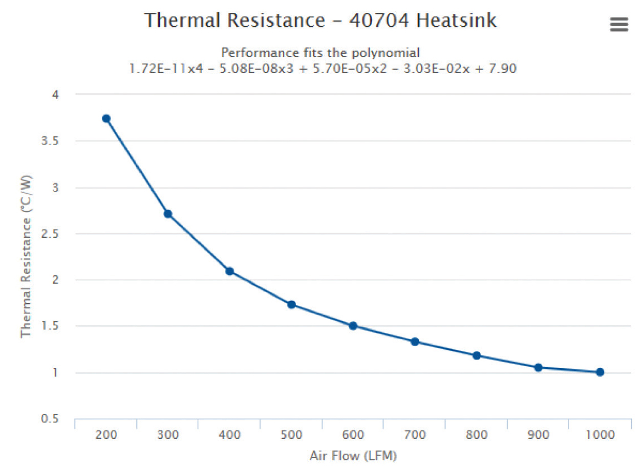 Figure 5: Thermal resistance graph and polynomial fit for 11mm P/N 40704 heatsink
The thermal circuit modelling technique outlined here provides a simple and useful design tool to develop and characterise an effective thermal management system for power components, without the need to acquire and learn to use more expensive thermal simulation software.
Product Spotlight
APV1111GVY
Panasonic

Panasonic PhotoMOS® Photovoltaic MOSFET High-Power Drivers
| SKU: | |
|---|---|
| Stock: | 3490 |
| Cost: | $3.95 |
