Switching ICs meet US DoE EPS efficiency regulations
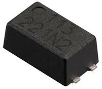
A series of switching ICs suitable for mobile devices which are subject to 30mW no-load limitations, has been released by Power Integrations. The LinkSwitch-3 series delivers primary-side regulation for chargers and adapters up to 10W, making them suitable for smartphones and tablets which are subject to upcoming mandatory US DoE EPS efficiency regulations and EU CoC Tier 2 guidelines.
These ICs simplify CV/CC charger designs by eliminating the need for opto-couplers and secondary-side control circuitry. Highly accurate output voltage and current regulation are provided by the switching ICs, which compensate for transformer and internal parameter tolerances along voltage variation from the AC line.
The LinkSwitch-3 series incorporate a 725V power MOSFET, an on/off-control state machine, a high-voltage switched current source for self-biasing, frequency jittering to minimise EMI, cycle-by-cycle current limiting and hysteretic thermal shutdown circuitry. As well as this, the ICs also feature selectable cable drop compensation for improved voltage tolerance over load.
Silvestro Fimiani, Senior Product Marketing Manager, Power Integrations, comments: “The smart mobile device market is highly dynamic; LinkSwitch-3 ICs meet all of the most challenging new requirements. In addition to 10W maximum output power, the new devices meet the anticipated US DoE efficiency regulations, the EU’s CoC 2016 Tier 2 guidelines, China’s USB charger specification and market demand for 30mW no-load performance with fast transient response.”


